Difference between revisions of "CoE 197U Memory"
| Line 13: | Line 13: | ||
Static memory rely on the principle of ''positive feedback'' to achieve two possible states, or what we call a bistable circuit, represented as either a 0 or a 1. Fig. 1 shows the basic idea of positive feedback, illustrated by 2 inverters connected in a ring. Considering the first inverter, the input is V<sub>i1</sub> and output is V<sub>o1</sub>, and the corresponding VTC is shown on the left. For the second inverter, the input is V<sub>i2</sub> = V<sub>o1</sub> and the output is V<sub>o2</sub> = V<sub>i1</sub>. So we can flip the VTC as shown on the right, so the axes of both plots coincide. As such, we can combine as shown on the figure at the bottom. Here we can see that we have 3 operating points: A (V<sub>i1</sub>=0, V<sub>o1</sub> = 1), B (V<sub>i1</sub> = 1, V<sub>o1</sub> = 0) and C. Point C is known as the metastable state. That is, assuming the inverter pair in Fig. 1 happens to be biased at point C, a small deviation or noise can shift to either point A or point B. This is illustrated in Fig. 2. A small deviation ''d'' gets amplified through the inverter pair causing the operating point to shift from C to A and stay at A. From either point A or B, however, even a larger deviation will not shift the operating point, making point A and B stable states. | Static memory rely on the principle of ''positive feedback'' to achieve two possible states, or what we call a bistable circuit, represented as either a 0 or a 1. Fig. 1 shows the basic idea of positive feedback, illustrated by 2 inverters connected in a ring. Considering the first inverter, the input is V<sub>i1</sub> and output is V<sub>o1</sub>, and the corresponding VTC is shown on the left. For the second inverter, the input is V<sub>i2</sub> = V<sub>o1</sub> and the output is V<sub>o2</sub> = V<sub>i1</sub>. So we can flip the VTC as shown on the right, so the axes of both plots coincide. As such, we can combine as shown on the figure at the bottom. Here we can see that we have 3 operating points: A (V<sub>i1</sub>=0, V<sub>o1</sub> = 1), B (V<sub>i1</sub> = 1, V<sub>o1</sub> = 0) and C. Point C is known as the metastable state. That is, assuming the inverter pair in Fig. 1 happens to be biased at point C, a small deviation or noise can shift to either point A or point B. This is illustrated in Fig. 2. A small deviation ''d'' gets amplified through the inverter pair causing the operating point to shift from C to A and stay at A. From either point A or B, however, even a larger deviation will not shift the operating point, making point A and B stable states. | ||
| − | [[File:Fig1-positive feedback.png|thumb|500px|Fig. 1 Positive Feedback]] | + | [[File:Fig1-positive feedback.png|thumb|center|500px|Fig. 1 Positive Feedback]] |
[[File:Fig2-metastable.png|thumb|500px|Fig. 2 Metastability]] | [[File:Fig2-metastable.png|thumb|500px|Fig. 2 Metastability]] | ||
| Line 19: | Line 19: | ||
One possible implementation of the latch is the mux-based, as shown in Fig. 3. Here, while CLK = 1, the lower transmission gate is closed, giving a direct path from D to Q. Once the CLK goes low, the lower transmission gate opens while the top transmission gate closes. Thus the path from D is disconnected while the data in Q gets stored through the inverter pair. | One possible implementation of the latch is the mux-based, as shown in Fig. 3. Here, while CLK = 1, the lower transmission gate is closed, giving a direct path from D to Q. Once the CLK goes low, the lower transmission gate opens while the top transmission gate closes. Thus the path from D is disconnected while the data in Q gets stored through the inverter pair. | ||
| − | [[File:Fig3-mux-based.png|thumb|500px|Fig. 3 MUX-based Latch]] | + | [[File:Fig3-mux-based.png|thumb|center|500px|Fig. 3 MUX-based Latch]] |
Dynamic latches store data through parasitic capacitances as shown in Fig. 4 on the left. However, the charge on the capacitance may be discharged especially of the clock period is long. As such some refreshing mechanism is needed to ensure that the charge in the capacitor is replenished and therefore data will not be lost. A possible solution to this is the peudo-static latch, where a small keeper inverter is added to provide the positive feedback for the data and therefore no refreshing is necessary. | Dynamic latches store data through parasitic capacitances as shown in Fig. 4 on the left. However, the charge on the capacitance may be discharged especially of the clock period is long. As such some refreshing mechanism is needed to ensure that the charge in the capacitor is replenished and therefore data will not be lost. A possible solution to this is the peudo-static latch, where a small keeper inverter is added to provide the positive feedback for the data and therefore no refreshing is necessary. | ||
Revision as of 18:31, 2 April 2021
In this lecture, we will cover the following topics:
- Classification of Memory
- Static and Dynamic Latches and Registers
- Pipelining
Use the provided slide deck to guide you through this discussion. The main reference for this lecture is the Digital IC book[1]
Memory Classification
Memory can be classified according to different categories. Memory can be either foreground (as part of logic, such as in sequential circuits) or background (as a large storage). Memory can also be classified as either static, that is the data is retained as long as power is ON, or dynamic, where constant refreshing of the data is needed. In sequential circuit, we can also classify memory as either a register (or sometimes referred as flip-flops, meaning edge sensitive) or a latch (meaning level sensitive).
Memory Elements
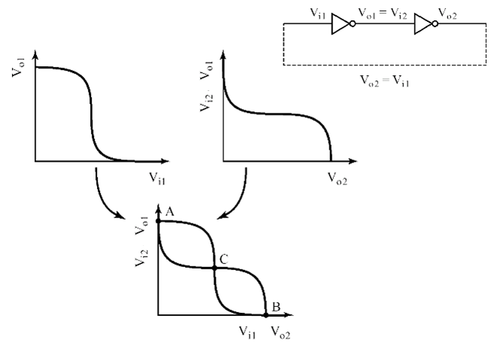
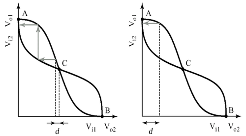
Static memory rely on the principle of positive feedback to achieve two possible states, or what we call a bistable circuit, represented as either a 0 or a 1. Fig. 1 shows the basic idea of positive feedback, illustrated by 2 inverters connected in a ring. Considering the first inverter, the input is Vi1 and output is Vo1, and the corresponding VTC is shown on the left. For the second inverter, the input is Vi2 = Vo1 and the output is Vo2 = Vi1. So we can flip the VTC as shown on the right, so the axes of both plots coincide. As such, we can combine as shown on the figure at the bottom. Here we can see that we have 3 operating points: A (Vi1=0, Vo1 = 1), B (Vi1 = 1, Vo1 = 0) and C. Point C is known as the metastable state. That is, assuming the inverter pair in Fig. 1 happens to be biased at point C, a small deviation or noise can shift to either point A or point B. This is illustrated in Fig. 2. A small deviation d gets amplified through the inverter pair causing the operating point to shift from C to A and stay at A. From either point A or B, however, even a larger deviation will not shift the operating point, making point A and B stable states.
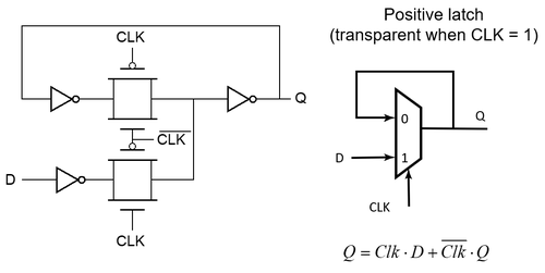
One possible implementation of the latch is the mux-based, as shown in Fig. 3. Here, while CLK = 1, the lower transmission gate is closed, giving a direct path from D to Q. Once the CLK goes low, the lower transmission gate opens while the top transmission gate closes. Thus the path from D is disconnected while the data in Q gets stored through the inverter pair.
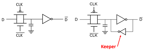
Dynamic latches store data through parasitic capacitances as shown in Fig. 4 on the left. However, the charge on the capacitance may be discharged especially of the clock period is long. As such some refreshing mechanism is needed to ensure that the charge in the capacitor is replenished and therefore data will not be lost. A possible solution to this is the peudo-static latch, where a small keeper inverter is added to provide the positive feedback for the data and therefore no refreshing is necessary.
Pipelining
References
- ↑ J. Rabaey, A. Chandrakasan, B. Nikolic, Digital Integrated Circuits, 2nd ed., 2002


