CoE 197U Timing
In this lecture, we will cover the following topics:
- Register timing basics
- Timing Uncertainty
- Clock distribution
Use the provided slide deck to guide you through this discussion. The main reference for this lecture is the Digital IC book[1]
Note that the slide deck contains information for both latch and register. In this discussion, we focus only on register timing.
Contents
Timing Basics
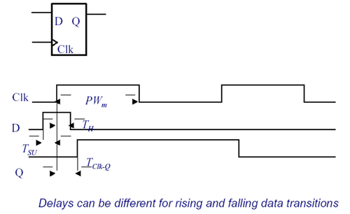
Shown in Fig. 1 is an illustration of the timing parameters of a register. Important parameters here are setup time (tsu), hold time (tH), clock-to-Q delay (tclk-q) and clock period (Tclk). Setup time is the minimum time required that the input data, D, has to be stable before the edge of the CLK. Hold time, on the other hand, is the minimum time required for data, D, to remain stable after the edge of the clock. The clk-to-q delay, as the name implies, is the time after the edge of the clock when the output, Q, is considered valid.
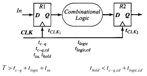
Given the register timing parameters, we can compute for the clock period and hold time constraints of a sequential circuit. This is illustrated in Fig. 2. Corresponding equations are also shown in the figure. Before defining the constraints, we define first a new term – contamination delay. Contamination delay (tcd) is the minimum time from when the input changes until any output starts to change. In this figure, we have defined 2 contamination delays: tc-q,cd (clk-to-q contamination delay) and tlogic,cd (combinational logic contamination delay). To define the minimum clock period, from the clk edge going to R1, data must be processed through the combinational logic and be ready for sampling by R2 before the next clock edge. Thus, the clock period, T, must be greater than clock-to-q delay of R1 plus the delay through the combinational logic plus the setup time of R2. For the hold time, we need to make sure that we satisfy the hold time for R2. So after the edge of clock arrives, the D input of R2 must not change for at least thold. The minimum delay from R1 to R2 is tc-q,cd plus tlogic,cd. So thold must be less than this value.
Timing Uncertainty
We consider 2 clock non-idealities or uncertainties here: skew and jitter. Skew is the difference in time between supposedly synchronous clock edges. It is caused by the delay in the clock signal due to routing. Clock jitter, on the other hand, is a temporal variation (varies over time) in consecutive clock edges. As a result, cycle-to-cycle clock period may actually vary. Fig. 3 illustrates these uncertainties. The CLK signal on top is supposed to be the same CLK signal at the bottom. Imagine the top clk signal goes to the clk signal of R1 (Fig. 2) while the bottom clk signal (which is supposedly the same as the top but delayed due to routing) goes to the clk of R2. Would the equations still hold? How will this impact the constraints on clock period and hold time? Notice also the uncertainty on the clock edges. This means that we are not sure when the edge exactly appears per cycle. To ensure that the design will always work, inspite of these uncertainties, we would need to design for the worst case. That is, we assume the edge that would give the worst performance.
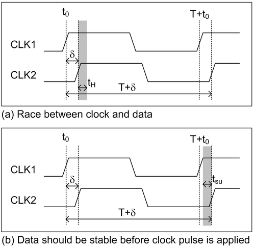
Let us then revisit the constraints, taking clock skew into consideration, using Fig. 4 as basis for the timing parameter. The launching register R1 in Fig. 2 is clocked at to while the capturing register R2 is clocked at to + δ. The data at the input of R2, therefore, has to be kept stable until to + δ + tH. Similarly, the sampling edge of the capturing register will be at T + to + δ. Thus, we get the following constraints (see slide 12 of provided slide deck for details):
- T > tc-q + tlogic + tsu + δ
- δ < tc-q,cd + tlogic,cd - tH
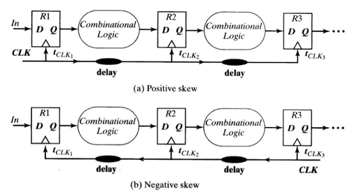
Note that skew may be positive or negative, as shown in Fig. 5. A skew is positive if the clock goes in the same direction as the data. This is what we illustrated in the previous slides. However, the clock may be routed in the opposite direction as the data. This is what we call the negative skew. Note in the figure that the capturing register is clocked before the launching register.
Considering jitter, being a temporal variation, we need to consider the worst case. That is, the clock period at worst case would always be T - 2tjitter. Consider the CLK signal in Fig. 6. The nominal clock period is from (2) to (5) of the figure as shown. The shortest clock period is from (3) to (4) of the figure. The largest possible period is from (1) to (6).
Read through the succeeding slides for the combined effect of jitter and skew.
Optional: Pipelining
Pipelining allows improvement of throughput by diving the whole process into several tasks, with each task expected to complete within a single clock cycle. This is illustrated in Fig. 6 below. The reference design completes all tasks in a single cycle. Of course, the clock period will be limited by how long all these processes will complete. The pipelined version inserts registers in between the different sub-tasks to avoid loosing data. Each sub-task will take one cycle, so the clock period will be limited by the slowest sub-task.An advantage of the pipelined version is that inputs a and b may be fed each clock cycle (which is ~3x faster than the reference) and therefore the effective throughput is faster.
Optional: Clock distribution
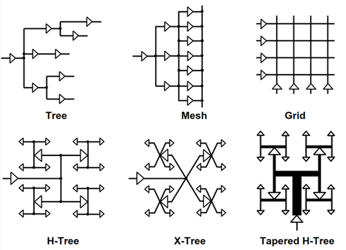
To help reduce skew between clock signals of registers, clock distribution has become an integral part in the implementation process of digital designs. Fig. 7 shows some common distribution networks used. Note that the actual delay from the clock pin to the clock input of the register does not matter -- it's the relative delays between clocks going into the register clock inputs that is important. Notice, for example, in the tree network, there is 3 inverter delays from the clock pin to the clock branches. However, since delays from pin to any branch takes 3 inverter delays, then the relative delay among those branches is minimal. Of course, if the load of those branches are different, then their relative delay will also differ. This is what the mesh tries to solve -- connect intermediate branches so they same the same load. The H-tree network is one of the more commonly used techniques to date. In this case, the clock is routed to the center, which is again routed to the center of each of the 4 quadrants. This continues until the load is already manageable.
References
- ↑ J. Rabaey, A. Chandrakasan, B. Nikolic, Digital Integrated Circuits, 2nd ed., 2002
