Difference between revisions of "CoE 197U Interconnects"
| (8 intermediate revisions by the same user not shown) | |||
| Line 7: | Line 7: | ||
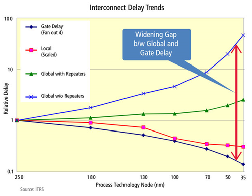
Wires are often neglected during design. They are simply used to connect signals from one point to another and assumed to have negligible effect on the performance of the system. Figure 1 shows the widening gap between wire delays and gate delays. As technology scales, dimensions and delays decrease. However, with the thinner interconnects, the wire resistance per unit length increases. As such, degradation in performance can be expected if they are not dealt with properly. | Wires are often neglected during design. They are simply used to connect signals from one point to another and assumed to have negligible effect on the performance of the system. Figure 1 shows the widening gap between wire delays and gate delays. As technology scales, dimensions and delays decrease. However, with the thinner interconnects, the wire resistance per unit length increases. As such, degradation in performance can be expected if they are not dealt with properly. | ||
| − | [[ File:Fig1-wires.png | + | [[File:Fig1-wires.png|center|thumb|500px|Fig. 1 Interconnect Delay Trends from ITRS report]] |
| − | In terms of models, interconnects are represented as parasitics the degrade performance and reduce reliability of the system. Classes of parasistics are capacitive, resistive and inductive. For this course, we consider mostly capacitive and resistive. Any two parallel conductors with a dielectric in between can be treated as a capacitor. This is illustrated in Figure 2 and the corresponding equation shown. Typical CMOS IC uses silicon dioxide as dielectric. The table | + | In terms of models, interconnects are represented as parasitics the degrade performance and reduce reliability of the system. Classes of parasistics are capacitive, resistive and inductive. For this course, we consider mostly capacitive and resistive. Any two parallel conductors with a dielectric in between can be treated as a capacitor. This is illustrated in Figure 2 and the corresponding equation shown. The parameter ''ε<sub>di</sub>'' if the permitivity of the dielectric. It is common to specify the relative permitivity, ε<sub>r</sub>, of a material. That is, '''ε<sub>di</sub> = ε<sub>r</sub>ε<sub>0</sub>''', where ε<sub>0</sub> is the permitivity of free space and is equal to 8.854x10<sup>-12</sup> F/m. Typical CMOS IC uses silicon dioxide as dielectric. The table below shows dielectric constants of other materials. |
| + | [[File:Fig2-capwire.png|center|thumb|650px|Fig 2. Parallel Plate Capacitance]] | ||
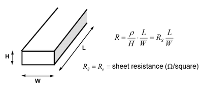
| + | Any material will have some resistance. The equation is given in Fig. 3 , with the corresponding dimensions illustrated. Since the height (H) of the material is dictated by the manufacturing process, and the conductivity (rho) is determined by the material, then we can separate the length and width from the other parameters. The simplest model for interconnects is the lumped model, where total capacitance and total resistance of the conductor is computed and treated as a single RC network. | ||
| − | + | [[File:Fig3-wire res.png|center|thumb|400px|Fig 3. Wire Resistance]] | |
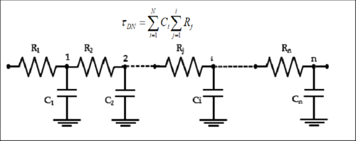
| + | For long wires, the interconnect can be viewed as cascaded shorter wires, each having its R and C., as shown in Fig. 4. The path delay is computed using the given equation. For a sample problem and solution, you may watch the video: https://www.youtube.com/watch?v=1c_AgRmXQBw. | ||
| − | + | [[File:Wire-delay-model-Elmore-Delay-formula.png|center|thumb|500px|Fig 4. Elmore Delay]] | |
| + | <big>[[CoE 197U Memory | Next: Memory]]</big> | ||
== References == | == References == | ||
Latest revision as of 20:16, 29 March 2021
In this lecture, we will cover topics on wires and interconnects.
Use the provided slide deck to guide you through this discussion. The main reference for this lecture is Chapter 4 of the Digital IC book[1]
Interconnects
Wires are often neglected during design. They are simply used to connect signals from one point to another and assumed to have negligible effect on the performance of the system. Figure 1 shows the widening gap between wire delays and gate delays. As technology scales, dimensions and delays decrease. However, with the thinner interconnects, the wire resistance per unit length increases. As such, degradation in performance can be expected if they are not dealt with properly.
In terms of models, interconnects are represented as parasitics the degrade performance and reduce reliability of the system. Classes of parasistics are capacitive, resistive and inductive. For this course, we consider mostly capacitive and resistive. Any two parallel conductors with a dielectric in between can be treated as a capacitor. This is illustrated in Figure 2 and the corresponding equation shown. The parameter εdi if the permitivity of the dielectric. It is common to specify the relative permitivity, εr, of a material. That is, εdi = εrε0, where ε0 is the permitivity of free space and is equal to 8.854x10⁻¹² F/m. Typical CMOS IC uses silicon dioxide as dielectric. The table below shows dielectric constants of other materials.
Any material will have some resistance. The equation is given in Fig. 3 , with the corresponding dimensions illustrated. Since the height (H) of the material is dictated by the manufacturing process, and the conductivity (rho) is determined by the material, then we can separate the length and width from the other parameters. The simplest model for interconnects is the lumped model, where total capacitance and total resistance of the conductor is computed and treated as a single RC network.
For long wires, the interconnect can be viewed as cascaded shorter wires, each having its R and C., as shown in Fig. 4. The path delay is computed using the given equation. For a sample problem and solution, you may watch the video: https://www.youtube.com/watch?v=1c_AgRmXQBw.
References
- ↑ J. Rabaey, A. Chandrakasan, B. Nikolic, Digital Integrated Circuits, 2nd ed., 2002


