Difference between revisions of "220-A3.1"
Jump to navigation
Jump to search
| Line 17: | Line 17: | ||
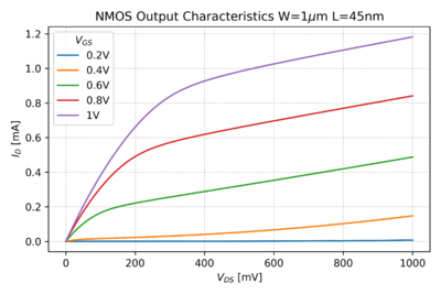
== MOS Output Characteristics == | == MOS Output Characteristics == | ||
| − | + | [[File:NMOS output tt.png|thumb|400px|Figure 4: The NMOS output characteristics.]] | |
== Activity: PMOS V-I Characteristics == | == Activity: PMOS V-I Characteristics == | ||
Revision as of 09:23, 16 October 2020
Activity: MOSFET Characteristic Curves
- Instructions: This activity is structured as a tutorial with an activity at the end. Should you have any questions, clarifications, or issues, please contact your instructor as soon as possible.
- At the end of this activity, the student should be able to:
- Generate the characteristic curves of NMOS and PMOS transistors.
MOS Transfer Characteristics
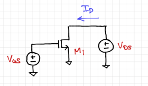
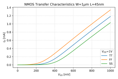
The transfer characteristics of an NMOS transistor is the relationship between the gate-source voltage, which serves as the "input" port of a common-source amplifier, and the "output" drain current. To simulate the transfer characteristic of our 45nm NMOS PTM model, we can use this SPICE file and this Python script.
To identify the different operating regions, we can
MOS Output Characteristics


