220-A3.1
Activity: MOSFET Characteristic Curves
- Instructions: This activity is structured as a tutorial with an activity at the end. Should you have any questions, clarifications, or issues, please contact your instructor as soon as possible.
- At the end of this activity, the student should be able to:
- Generate the characteristic curves of NMOS and PMOS transistors.
Contents
MOS Transfer Characteristics
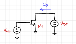
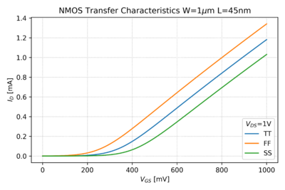
The transfer characteristics of an NMOS transistor is the relationship between the gate-source voltage, which serves as the "input" port of a common-source amplifier, and the "output" drain current. To simulate the transfer characteristic of our 45nm NMOS PTM model (TT, FF, SS), we can use this SPICE file and this Python script.
Activity 1: MOS Operating Regions
Use the given SPICE file and Python script to plot out the NMOS transfer characteristics, as shown in Figs. 2 and 3. Graphically, identify the following regions:
- The quadratic or square-law region
- The velocity saturation region
- The subthreshold or weak inversion region
- The moderate inversion region.
Change to 0.5V and 0.25V. Comment on the effect of process variations and changing on the transfer characteristics, specifically the value of the drain current, and the operating regions. Note that to enable the altermod command to change the model file, the full path of the model file must be specified.
Activity 2: NMOS Output Characteristics
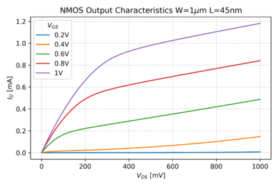
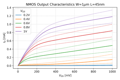
The given SPICE file and Python script also plots the NMOS output characteristics, shown in Fig. 4. Fig. 5 shows the effect of variations, showing the increased current of the FF corner and the lower current of the SS corner in dotted lines. Plot the NMOS output characteristics and graphically, identify the saturation region, the subthreshold region, and the linear or resistive region. Comment on the effect of process variations.
Activity 3: PMOS V-I Characteristics
Create a circuit to generate the transfer and output characteristics of a 45nm PMOS transistor (TT, FF, SS), similar to the NMOS plots above, also with and . Then repeat activities 1 and 2.
Report Guide
Write up a 2-3 page report with the annotated graphs showing the different regions of operation for both the NMOS and PMOS transistors, and submit the report via email.


