CoE 197U Logical Effort
In this lecture, we will cover the following:
- Delay Parameters
- Logical Effort of Simple Gates
- Multistage Networks
Use the provided slide deck to guide you through this discussion. The main reference for this lecture is Sutherland's book[1] and paper[2].
Delay
The delay of a path is equal to the sum of individual gate delays and the delay through the interconnect lines. Each gate delay can be decomposed into its intrinsic delay, p, and the effort delay, f. The effort delay is given by f = gh, where g is the logical effort and h is the effective fanout = Cout / Cin.
Logical Effort
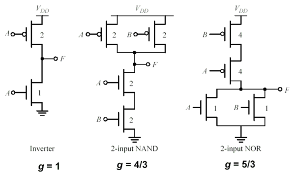
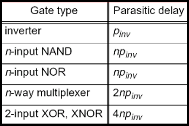
Logical effort is a function of the gate topology and is independent of sizing. It represents the ratio of its input capacitance to the inverter capacitance when size to deliver the same current. The logical effort of the INV, NAND2 and NOR2 are shown in Fig. 1. The simplest gate is the inverter, with an input capacitance of 3Cmin (2Cmin from pmos and Cmin from nmos). For the NAND2, each input sees 2Cmin from pmos and 2Cmin from nmos, giving a logical effort g = 4/3. The logical effort of other static CMOS gates is shown in Table 1. The parasitic delays of static CMOS gates are shown in Table 2.
Multistage Networks
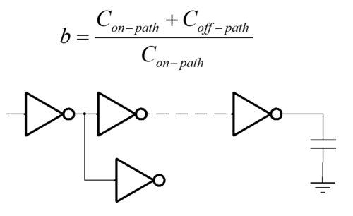
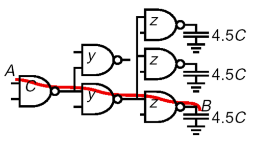
For multistage networks, or paths with cascaded gates, assuming negligible interconnect delay, the delay will be the sum of individual delays of the gates along the path. Using logical effort, we can also optimize the delay through proper sizing of gates. An additional parameter we need to add is the branching effort. Branching effort takes into account the additional capacitive load contributed by paths branching off from the path in consideration. This is illustrated in Fig. 2 below.
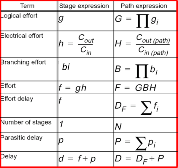
Refer to Table 3 below for a summary of terms and equations in solving delays for multistage networks.
Given a multistage network such as that shown in Fig. 3, we start by computing or determining the path electrical effort, H, stage logical effort, g, and path logical effort, G, computed as the product of individual stage logical effort. Since there are paths branching off from the path being optimized, stage and path branching effort will also need to be computed. The total path effort is then defined as F = GHB. For optimal delay, the effort delay per stage should be equal. See slide 15 of the provided slide deck for the complete solution of this problem.
