220-A1.2
- Activity: Simulating simple RLC circuits
- At the end of this activity, the student should be able to:
- Run DC, AC, and transient simulations using ngspice.
Contents
A Wideband RC Voltage Divider
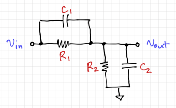
One way to build high-speed circuits with relatively large input impedances and capacitances is to use a simple RC voltage divider, as shown in the figure below. This RC divider is commonly found in oscilloscope 10X probes.
Let and similarly . Thus, the output voltage can be expressed as:
-
(1)
-
Notice that we can cancel out the pole with the zero when we set , or equivalently,
-
(2)
-
Intuitively, we can think if this as a resistive voltage divider at low frequencies, and a capacitive divider with the same ratio at high frequencies. Thus, the output voltage will simply be equal to:
-
(3)
-
We can then build a simple 10X oscilloscope probe circuit with an input impedance of and an input capacitance of using , , , and . Since the pole and zero cancel each other out, the bandwidth of the probe circuit is not limited by its RC values.
Let's look at the frequency response and transient response of this circuit using ngspice.
Simulating the RC Voltage Divider
Let us start with the SPICE netlist below, where we will analyze this piece by piece.
Line 1 is always reserved for the circuit title, and in this case, it is followed by a comment. The .options directive follows, telling the simulator to save the device current data for later printing or plotting.
1 * Wideband Voltage Divider Circuit
2 * LPA 05 Aug 2020
3
4 .options savecurrents
The next few lines describe our wideband voltage divider, composed of the resistors , , , and .
 6 R1		in out		900k
 7 R2		out 0		100k
 8
 9 C1		in out	 	1.1111p
10 C2		out 0		10p
11
12 * increase C1 and see what happens
13 R1a		in outa		900k
14 R2a		outa 0		100k
15
16 C1a		in outa	 	1.6p
17 C2a		outa 0		10p
18
19 * decrease C1 and see what happens
20 R1b		in outb		900k
21 R2b		outb 0		100k
22
23 C1b		in outb	 	0.7p
24 C2b		outb 0		10p
25
26 * input square wave
27 V1		in 0		dc 1 ac 1 pulse(-1 1 0 0.1u 0.1u 5u 0.01m)
28
29 .control
30
31 ac dec 10 1 1G
32 plot vdb(out) vdb(outa) vdb(outb)
33 wrdata testac.dat v(out) v(outa) v(outb)
34
35 tran 0.01u 0.03m
36 plot v(out) v(outa) v(outb)
37 wrdata testtran.dat v(out) v(outa) v(outb)
38
39 .endc
40
41 .end
Notice that we described three copies of the same circuit, but with different values of . Lines 6-10 describe circuit 1, while lines 13-17 and 20-24 describe circuits 2 and 3 respectively, with the following values of : , , and . The three circuits all have the same ideal input voltage source, V1.


