CoE 197U Two-Stage MOS Operational Transconductance Amplifiers
If a larger gain than that of a differential amplifier is needed, the next step is to use cascade amplifier stage/s or cascode the differential pair. Cascoding uses common-gate amplifiers/buffers to increase gain at the cost of reduced voltage swing. Meanwhile, cascading can achieve larger voltage swings but need separate current paths and therefore, consume more power. With nominal supply voltages decreasing with technology, cascoding becomes less viable. In this lecture, we will look at a typical 2-stage MOS amplifier.
The main reference for this topic is chapter 6.3 of the Analysis and Design of Analog Integrated Circuits book[1].
Contents
Op-amps and OTA
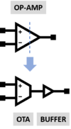
An operational amplifier or op-amp can be roughly divided into three stages (Fig. 1): the differential pair, the gain stage/s, and the output stage. The differential pair enables the op-amp to have a differential input, have a large input resistance, and provide some gain. The gain stage/s provide the additional gain needed, but in doing so, end up with a large output resistance that cannot drive heavy (low resistance) resistive loads. The output stage provides a gain of 1 or less. It is added to give the op-amp low output resistance, large output swing, and the ability to provide large output currents.
The differential and gain stages combined can be viewed as an OTA or operational transconductance amplifier. Thus, the op-amp can be viewed as an OTA with an output buffer (Fig. 2). OTAs have large gain and large output resistance. An OTA produces an output current from an input voltage and can drive capacitive loads (provide charging current) which are common in on-chip loads (e.g. gate of another MOSFET). A low output resistance is not necessarily required in driving capacitive loads.
Miller OTA
The Miller OTA is a simple 2-stage OTA composed of a current mirror-loaded differential pair stage and a common source stage (Fig. 3). It is one of the go-to amplifiers in IC design because of its simplicity. The topology contains only a few transistors, making it relatively easy to design. The circuit also has a simple biasing scheme. The design of the current source itself is a different story! However, in less critical applications, a resistor can be used in place of the current source. There are many problems associated with the latter scheme. On-chip resistors are not accurate, may occupy large chip area, can change resistance with temperature, and provides current that is sensitive to temperature and supply voltage changes.
This two-stage OTA can be compensated by using a compensating capacitor, . Compensation is needed to ensure that the amplifier is stable when used in feedback. You may refer to these materials[2] to review the fundamental concepts of feedback and compensation. If the load capacitance is not large enough to create a dominant pole, then the capacitor can be added. Placing a very large capacitor to produce a dominant pole is expensive in terms of chip area. By placing the capacitor as shown, a smaller capacitance value (and thus area) is needed since the Miller effect amplifies the capacitance by a factor . This amplified capacitance effectively appears at the input of the common source stage (or output of the differential pair) to ground. With a large enough , the pole associated with the output of the differential pair can be made dominant to ensure stability.
Before proceeding, note that the analysis to be presented assumes that all transistors are saturated square law devices described by the equations below (for NMOS). The term overdrive voltage or is used to refer to or . For PMOS devices, refers to . The paired devices (M1 and M2, and M3 and M4) have the same dimensions. All NMOS transistors are also assumed to have the same threshold voltage while all PMOS transistors are assumed to have the same threshold voltage .


