CoE 197U The CMOS Inverter
Revision as of 12:41, 10 March 2021 by Louis Alarcon (talk | contribs)
To understand the analysis and design of digital circuits, we will look at its fundamental element -- the digital gate. We will start with the simplest digital gate, the inverter.
Contents
The Inverter Voltage Transfer Characteristics (VTC)
The functionality of the inverter can be captured by looking at the output voltage as we change the input voltage, or the voltage-transfer characteristic (VTC).
The Ideal Inverter VTC
Let us define an ideal inverter, where the output voltage, is logic 1 or high when the input voltage, is less than a reference voltage, .
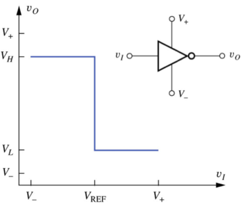 Figure : The ideal inverter voltage transfer characteristic (VTC)[1]. |
Static Design Metrics
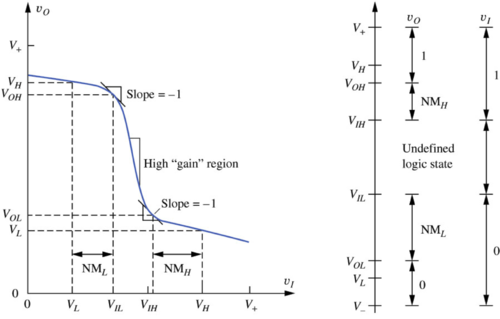 Figure : The non-ideal inverter voltage transfer characteristic (VTC)[1]. |
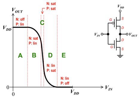 Figure : The CMOS inverter voltage transfer characteristic (VTC)[2]. |
Noise in Digital Circuits
Noise Rejection
Noise Margins
The Regenerative Property of Inverters
Inverter Delay
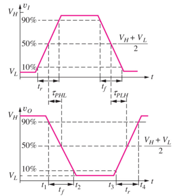 Figure: Logic delay definitions [1]. |
Power Dissipation
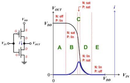 Figure : The CMOS switching current[3]. |
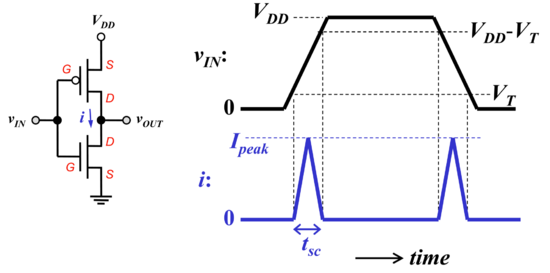 Figure : The CMOS transient power dissipation[3]. |
Energy Consumption
References
- ↑ Jump up to: 1.0 1.1 1.2 Ming Wu's UCB EE105 (Fall 2014) Lecture 24 Slides (link)
- ↑ Tsu-Jae King's UCB EECS40 (Fall 2003) Lecture 26 Slides (link)
- ↑ Jump up to: 3.0 3.1 Tsu-Jae King's UCB EECS40 (Fall 2003) Lecture 27 Slides (link)


