CoE 197U The MOS Switch
Contents
Levels of Abstraction
As integrated circuits continue to increase in complexity and sophistication, the amount of information and information processing needed to design, fabricate, and test these ICs also increase. Without a way to organize this information, engineers can be easily overwhelmed. One strategy is to define levels of abstraction, where we partition the information, and use only the components needed for a particular task. This strategy can then be used to create models appropriate for a certain objective.
We create models to allow us to predict the behavior of a circuit or system. One approach we can take is to model a whole system using transistor models, e.g. BSIM[1] models, with hundreds of parameters per transistor. The amount of computing resources needed for systems with millions of transistors could render this approach impractical.
In most cases, the overall functionality of a digital system is determined by the system architecture and organization, e.g. is it an adder, or a multiplier, or a microprocessor? At this level, we do not really need to know transistor-level details such as the threshold voltage or the thickness of the gate oxide. Thus, we can abstract away the unneeded information, and retain only the information needed to accomplish the task. By reducing the complexity of the transistor model, we can significantly reduces the amount of computation needed to verify the functionality of the digital system. However, if we want to predict or determine the leakage power consumption of the system, then we need to take into account the transistor threshold voltages, leading to a different simulation strategy and transistor model abstraction.
Fig. 1 shows an example of how a system can be seen from different levels of abstractions or viewpoints, from the system-level, to the RTL- or functional-level, the gate-level, the transistor-level, and the physical-level. Different models with varying sophistication and complexity can be used at the different levels, depending on the design or verification objective. In general, more information about the transistors are added as we get closer to the physical-level.
 Figure 1: Levels of abstraction[2]. |
For example, at the system-level, we may be interested in overall functionality of the IC and how it interfaces with other components or systems. At the register transfer level (RTL), we might be concerned with the system architecture, e.g. how it uses resources such as memory and interconnect to implement its function. Then each function could be examined in more detail at the gate-level, we can evaluate gate fan-in and fan-out, logic depth, etc. At the transistor-level, we can look at specific timing-, voltage- and current-related parameters such as rise times, propagation delays, voltage and current spikes, active and leakage power, etc. The physical-layer view can show us the effect of the layout and location of transistors and transistor groups, allowing us to determine the effects of parasitic elements and other layout related phenomena.
To understand the functionality of digital systems, let us first consider the functionality and performance of the simplest of all digital CMOS gates -- the inverter. We will see that we can easily extend these to more complex gates. Since we only want to look at CMOS inverters from a digital point of view, let us see if we can create a simple model for our transistors that is appropriate for this task.
Digital Transistor Operation
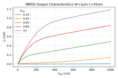
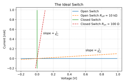
In digital circuits, the inputs and outputs are ideally limited to two voltage levels, usually or logic 1 and ground or logic 0. Fig. 2 shows the output characteristic of an NMOS transistor. Note that for large , e.g. 1V, the vs. characteristic of the NMOS transistor, at low , looks very much like a closed switch with a low series resistance, as seen in Fig. 3. Similarly for low , e.g. 0V, the NMOS transistor looks like an open switch.
 Figure 2: The 45nm NMOS PTM[3] output characteristics. |
The Switch Model of a Transistor
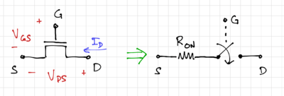
We can then think of an NMOS transistor as a voltage-controlled switch controlled by the gate-to-source voltage, as seen in Fig. 4. Thus, for , the switch is closed and as seen in Fig. 2, for , the on-resistance, can be modeled as the NMOS resistance in the triode region. When , we can model the NMOS transistor as an open switch.
We will see later on that we can modify these model parameters to determine other metrics in addition to functionality.
Note that the source terminal is always at a lower voltage compared to the drain terminal. Since the MOSFET is symmetric, the source and drain terminals could swap places if changes polarity. For PMOS transistors, since the threshold voltage is negative, the gate must be lower than the source voltage by at least a threshold voltage to turn on the PMOS switch.


