CoE 197U CMOS Gates
In this lecture, we will cover the following:
- Review of combinational logic
- CMOS gate sizing
- Designing for speed
Use the provided slide deck to guide you through this discussion. The main reference for this lecture is Chapter 6 of the Digital IC book[1].
Combinational Logic Review
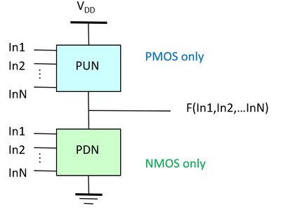
Combinational logic funstions are functions whose output value/s depend only on the current input values. They are typically expressed as Boolean functions, truth tables or logic gate networks. Common logic gates used are inverters (as discussed in previous lecture), AND gates, NAND gates, OR gates, NOR gates, etc. Static complementary gates are implemented using complementary (or dual) networks: a pull-up network (PUN) composed of PMOS transistors and a pull-down network (PDN) composed of NMOS transistors. The simplest of these gates is the inverter, where the PUN is a single PMOS and the PDN is a single NMOS, as shown in figure 1. Slide 5 also shows the corresponding layout (middle figure) and stick diagram (right figure) of an inverter.
CMOS Logic Gates
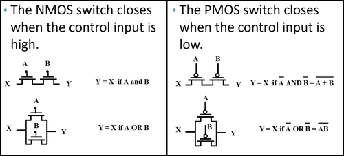
To design these logic gates, we can treat the transistors as controlled switches, similar to how we analyzed the inverter. We recall that NMOS switch closes when the control is HIGH, while PMOS switch closes when the control input is LOW. Connecting them in series or in parallel performs the logic as shown in figure 2.
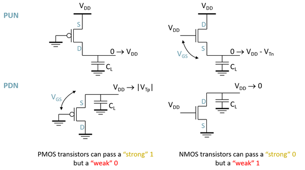
One thing we need to remember is that the PUN is composed of PMOS transistors ONLY while the PDN is composed of NMOS transistors ONLY. The reason for this is because PMOS transistors produce "strong 1's" while NMOS transistors produce "strong 0's" as illustrated in figure 3 below. As such, to have a full rail-to-rail output, we use the PUN (with PMOS transistors) to drive the output to '1' (VDD) and the PDN (with NMOS transistors) to set the output to '0' (GND).
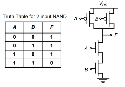
To construct a NAND gate, we can start from the truth table (shown in the figure below). The output will be '0' if both inputs (A and B) are HIGH. Since we need the output to be '0', we use the PDN and since both have to be high (at the same time), then we connect the NMOS transistors in series. In the same manner, the output will be '1' if either (or both) of the inputs are LOW. So using the PUN, since only one of the inputs need to be LOW, we connect them in parallel. Thus the NAND gate implementation as shown in figure 4 below. Slide 11 will show the implementation of the NOR gate.
Note that the PUN and PDN are duals. Being duals, transistors in parallel in the PUN will be in connected in series in the PDN and vice versa. For more complex gates, such as that shown in slide 12, we can start with either the PUN or the PDN, and connecting transistors (one at a time) either in series or in parallel. To produce a more compact layout, we could use the Euler's method to determine how to arrange the transistors. Watch this video for the step by step discussion of the slides.
Designing for Speed
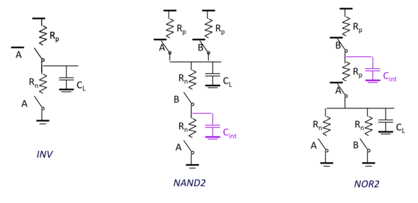
To estimate or compare delays of logic gates, we go back to the switch delay models of transistors, as we have done with inverters. Recall that a transistor can be modeled as a controlled switch with parasitic ON resistance and some capacitance. The switch delay models for the INV, NAND and NOR are shown in figure 5 below.
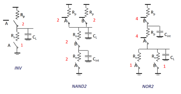
Let us consider first the NAND2 (2-input NAND) gate. For the output to be LOW (PDN is active), both NMOS transistors will be ON. In which case, we will see 2 resistances in series (total resistance will be the sum of both resistances). Thus, the high-to-low propagation delay, tP,HL, will be 0.69*2*RnCL. To switch the output from low to high, however, we can either have just a single ON transistor or both of them could be ON. In which case, we have 2 possible delays: (1) if only one transistor is ON, tP,LH = 0.69*RpCL; and (2) if both transistors are ON, tP,LH = 0.69*2*RpCL. To deal with this, we consider the worst case delay and size the transistors such that the PUN and PDU will have equal drive strength and therefore equal delay.
We can a similar analysis with the NOR2, except this time, the low-to-high propagation delay will be tP,LH = 0.69*2*RpCL and the worst case high-to-low propagation delay will be when only one of the transistors is ON and tP,HL = 0.69*RnCL. The proper sizing for the gates will then be as shown in Fig. 6.
References
- ↑ J. Rabaey, A. Chandrakasan, B. Nikolic, Digital Integrated Circuits, 2nd ed., 2002
