Passive CMOS Devices
Passive devices such as resistors, capacitors, and inductors, are commonly used in biasing circuits, feedback networks, and signal or energy storage blocks. However, these passive devices, when built on fabrication processes that are optimized for transistors, may have characteristics different from their ideal or discrete counterparts. In this module, we examine the behavior of passive devices built alongside CMOS transistors.
Contents
Resistors
In standard digital CMOS processes, there is usually no provision for high resistance layers, since resistances are typically deemed bad for digital circuits. But in analog design, we often need well-controlled resistors, with relatively large resistance values.
Sheet Resistance
In order to evaluate if a particular layer could be used as to build a resistor, we look to their sheet resistance. Recall that for a resistor:
-
(1)
-
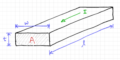
Where is the sheet resistance of the layer, is the resistivity of the material, is the length along the direction of the current, and , is the cross sectional area normal to the current flow, which is equal to the product of the layer thickness, and is the width of the layer perpendicular to the current flow, as shown in Fig. 1. Note that the resistivity, , and layer thickness, are technology specific parameters, and are determined by the fabrication process. The designer can specify resistance values by controlling the width, , and the length, .
Note that the units of sheet resistance is since is the resistance of a square, i.e. when . Table 1 shows indicative sheet resistance values of the common conductive layers in a CMOS process.
| Layer | Sheet Resistance |
|---|---|
| Metal | |
| Polysilicon | |
| or Diffusion | |
| -well |
An illustrative cross-section of resistors using these layers are shown in Figs. 2 and 3.
 Figure 2: Resistors built using semiconductor layers[1]. |
 Figure 3: Resistors built using metal layers[1]. |

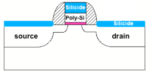
In a CMOS process optimized for digital circuits, the low sheet resistances of the semiconductor layers are due to a low-resistance silicide layer deposited on top of the semiconductor layer, as shown in Fig. 4. In analog CMOS processes, we are usually given the option to place a silicide block, i.e. to prevent the silicide layer from being deposited on specific locations on the die. Table 2 contains illustrative values of the sheet resistance of the semiconductor layers with the silicide block option.
| Layer | @ | |||
|---|---|---|---|---|
| -polysilicon | 100 | -800 | 50 | 50 |
| -polysilicon | 180 | 200 | 50 | 50 |
| -diffusion | 50 | 1500 | 500 | -500 |
| -diffusion | 100 | 1600 | -500 | 500 |
| -well | 1000 | -1500 | 20,000 | 30,000 |
Temperature and Voltage Coefficients
In general, semiconductor resistor values change with temperature and applied voltage, and to describe these changes, we use temperature and voltage coefficients:
-
(2)
-
Where is the nominal resistance value at some reference temperature , is the temperature coefficient, is the voltage coefficient, is the body voltage coefficient, and are the terminal voltages, and is the bulk or body or substrate voltage.
In semiconductors, we know that the resistivity is a strong function of temperature, roughly due to two mechanisms: (1) increasing the temperature increases the number of free carriers, thus lowering the resistance, resulting in negative temperature coefficients, and (2) this increase in free carriers increases the probability of scattering events or collisions, increasing the effective resistance, resulting in positive temperature coefficients. Thus, depending on which mechanism is dominant, we get positive or negative temperature coefficients.
The voltage coefficient models the changes in resistance values due to the varying depletion region widths caused by the terminal voltages. On the other hand, for the body voltage coefficient, we use the average voltage across the resistor relative to the substrate voltage.
Resistor Matching
Due to the nature of the manufacturing process steps such as photolithography, chemical and plasma etching, and ion implantation or diffusion doping, the layer dimensions and resistivity could change across wafers, across dies, or even across devices. Collectively we call these changes process variations, and if we are not careful, these variations could degrade the functionality and performance of our circuits. If we lump process variations with voltage and temperature changes, we refer to these as PVT variations.
We can classify process variations as either systematic or random.
- Systematic variations are deterministic variations, i.e. we can predict the changes. This could be due to the manufacturing process such as the existence doping or thickness gradients that results in one side of the wafer having thicker layers which gradually thin out as we get to the other side.
- Random variations are due to random processes such as electron diffusion, or photon scattering that creates random 'mismatch between devices. Though we cannot predict the actual values that arise from random processes, we can still describe, analyze, and design circuits based on the statistics, such as the mean and variance, of these random variables.
As we see in Table 1, the process variations in resistor values can be as large as . However, if we use ratios of resistors instead of their absolute values, together with good design and layout, we can reduce the mismatch, and in some cases to as low as .


![{\displaystyle R_{\mathrm {sh} }\,\mathrm {[\Omega /\square ]} }](https://en.wikipedia.org/api/rest_v1/media/math/render/svg/c0015b603c3b234abd2a81537a293d1230174e9a)
![{\displaystyle T_{C}\,\mathrm {[ppm/^{\circ }C]} }](https://en.wikipedia.org/api/rest_v1/media/math/render/svg/04b91e8231c6b3dfb9f275182a37fa14a115d0b4)

![{\displaystyle V_{C}\,\mathrm {[ppm/V]} }](https://en.wikipedia.org/api/rest_v1/media/math/render/svg/2999d120b9c9f1a9b2dffbdfb528de8b30f600a1)
![{\displaystyle B_{C}\,\mathrm {[ppm/V]} }](https://en.wikipedia.org/api/rest_v1/media/math/render/svg/4c9b77494824b8b10e640e2a1c937739746f56ee)
![{\displaystyle R=R_{0}\left[1+T_{C}\left(T-T_{0}\right)+V_{C}\left(V_{1}-V_{2}\right)+B_{C}\left({\frac {V_{1}+V_{2}}{2}}-V_{B}\right)\right]}](https://en.wikipedia.org/api/rest_v1/media/math/render/svg/4dcca9bfc0e25a572af319c1d76b0f841419492f)


