Introduction to EE 229
Welcome to EE 229!
Since we are offering this class remotely, there will be many changes to our normal course delivery:
- There will be no face-to-face lecture classes. All the material will be made available via this site.
- There will be more emphasis on student-centric activities, e.g. analysis, design, and simulations. Thus, you will be mostly "learning by doing". In this context, we will set aside an hour every week for consultations and questions via video-conferencing.
- Grades will be based on the submitted deliverables from the activities. Though we will not be very strict regarding the deadlines, it is a good idea to keep up with the class schedule and avoid cramming later in the semester.
Let's get started!
Contents
The Design of RF Transceivers

The objective of an RF transceiver is to transmit and receive information. To perform this task, however, requires concepts, technologies, and interactions from and among many fields, and some of these fields might not directly related to IC design. The task itself is relatively complex, with trade-offs and optimizations spanning various domains and levels of abstractions.
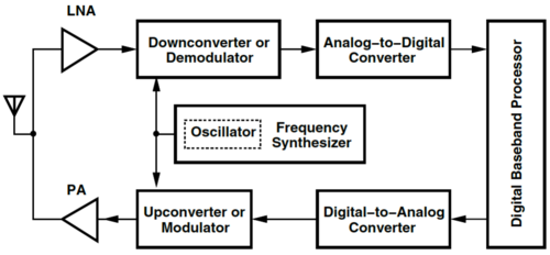
Fig. 1 shows a generic RF transceiver block diagram, showing:
- The transmit path, showing of basic system components needed to convert digital data into its analog form, modulate the signal, up-convert it from baseband to some center frequency, and finally send it to the antenna using a power amplifier.
- The receive path, where the signal is detected the low-noise amplifier, then down-converted back to baseband from a certain center frequency, then converted into the appropriate digital representation in preparation for further processing.
A Short Review
The goal of this module is to review the basic concepts of RF design, leading our coverage of communication systems, and then to transceiver architectures. These concepts and ideas will serve as the backdrop for analysis and design of RF circuits, allowing us to optimize our circuits for specific environments, contexts, and situations.
Power and Gain
The RF receiver subsystem is normally designed to detect and amplify signals that are at low power and voltage levels, while the transmitter subsystem is designed to deliver a sufficient amount of power to the antenna, enough to be detected at the remote receiver. Thus, we are very interested in the power and voltage gains of the blocks. Since we deal with a very large range of values, from microwatts for receivers to hundreds of watts for transmitters, it becomes convenient to express the voltage and power gains in terms of decibels (dB).
-
(1)
-
Time Variance
References
- ↑ Behzad Razavi, RF Microelectronics (2nd Edition), Prentice Hall Press, 2011, USA.
