CoE 197U The CMOS Inverter
From Microlab Classes
Revision as of 18:51, 5 March 2021 by
Louis Alarcon
(
talk
|
contribs
)
(
→Inverter Delay
)
(
diff
)
← Older revision
|
Latest revision
(
diff
) |
Newer revision →
(
diff
)
Jump to navigation
Jump to search
Contents
1
The Inverter Voltage Transfer Characteristics (VTC)
1.1
The Ideal Inverter VTC
2
Static Design Metrics
3
Noise in Digital Circuits
3.1
Noise Rejection
3.2
Noise Margins
3.3
The Regenerative Property of Inverters
4
Inverter Delay
5
Power Dissipation
6
Energy Consumption
7
References
The Inverter Voltage Transfer Characteristics (VTC)
The Ideal Inverter VTC
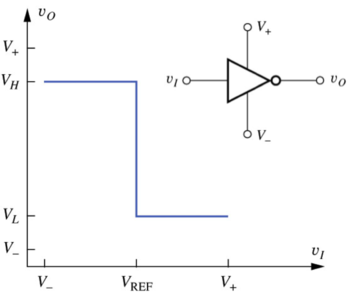
Figure : The ideal inverter voltage transfer characteristic (VTC)
[1]
.
Static Design Metrics
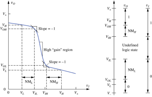
Figure : The non-ideal inverter voltage transfer characteristic (VTC)
[1]
.
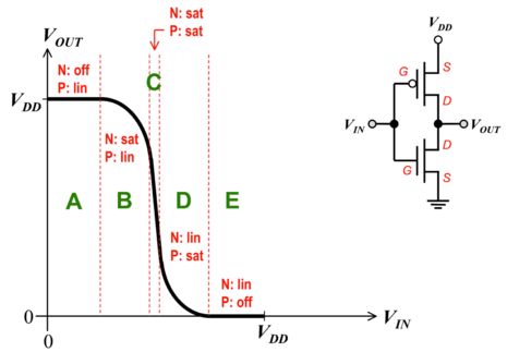
Figure : The CMOS inverter voltage transfer characteristic (VTC)
[2]
.
Noise in Digital Circuits
Noise Rejection
Noise Margins
The Regenerative Property of Inverters
Inverter Delay
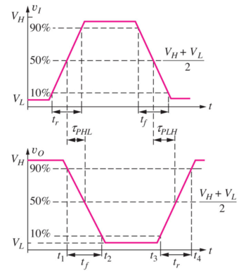
Figure: Logic delay definitions
[1]
.
Power Dissipation
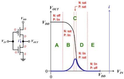
Figure : The CMOS switching current
[3]
.
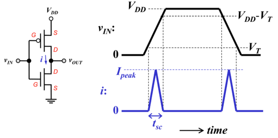
Figure : The CMOS transient power dissipation
[3]
.
Energy Consumption
References
↑
1.0
1.1
1.2
Ming Wu's UCB EE105 (Fall 2014) Lecture 24 Slides (
link
)
↑
Tsu-Jae King's UCB EECS40 (Fall 2003) Lecture 26 Slides (
link
)
↑
3.0
3.1
Tsu-Jae King's UCB EECS40 (Fall 2003) Lecture 27 Slides (
link
)
Navigation menu
Personal tools
Log in
Namespaces
Page
Discussion
Variants
Views
Read
View source
View history
More
Search
Navigation
Main page
Recent changes
Random page
Help about MediaWiki
Tools
What links here
Related changes
Special pages
Printable version
Permanent link
Page information
Cite this page