CoE 197U The MOS Transistor
Analog circuits are generally sensitive to the nuances and details of transistor behavior, requiring precise and/or well-controlled voltages, currents, etc. Digital circuits, on the other hand, can have much larger margins of error due to their inherent noise margins and regenerative properties. Thus, we want to be able to model these nuances and details of transistor behavior in order to predict their effects on our circuits.
Contents
Transistor Models
Transistor models enable us to describe and predict the behavior of the circuits we build using these transistors by:
- Providing us with a window into the physical device characteristics (e.g. dimensions, material and device properties, etc.) and processes (e.g. drift/diffusion currents, tunneling, charge transfer, etc.), and
- Allowing us to perform easy to do "experiments" using simulators such as SPICE[1].
Levels of Abstraction
The complexity of transistor models can range from very simple models, such as modeling the transistor as a simple controlled switch, to very complex models such as BSIM[2] models with hundreds of parameters.
We choose a model based on the questions we want answered. For example:
- For predicting the digital (boolean) functionality of a static CMOS gate, we can simply model the transistor as a controlled switch.
- However, if we want to predict the performance of the CMOS gate, we might need to model the ON current of the transistor as a current source in series with a switch.
- For high-precision analog circuits, we might need a BSIM model to predict the noise performance, settling time, stability, etc.
Note that "questions" that are more complicated require more complex and mathematically intensive models. Thus, it is best to match the model complexity to the problem or question we want answered. Further note that different models can be used to answer different questions at different stages of the design process.
The Square-Law MOSFET Model
The widely known square-law MOSFET model is a good model for predicting the behavior of discrete and relatively large-sized transistors. It relates the drain saturation current to the gate-to-source voltage as:
-
(1)
-
Where is the electron mobility, is the gate-oxide capacitance per unit area, dependent on the permittivity and thickness of the gate oxide layer, and is the transistor threshold voltage.
However, the square-law model is inadequate for modeling short-channel behavior, since it is based on the following assumptions (not a complete list):
- The channel charge density is determined only by the vertical electric field due to .
- Drift velocity is set only by the lateral electric field due to .
- The mobility of electrons and holes are constant.
- There are no diffusion currents, and that when .
Submicron Transistors
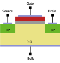
Due to manufacturing constraints and limitations, the structure of a deep submicron (with channel lengths of 90nm and below) transistors can differ quite dramatically from the idealized structure shown in Fig. 1. For an simple overview of the CMOS fabrication process, you can watch Silicon Run I (1996).
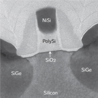
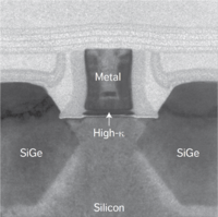
The cross section of modern MOSFETs with lengths of 90nm, 65nm, and 45nm are shown in Figs. 2, 3 and 4.
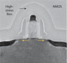 Figure 2: Intel 90nm MOSFET with tensile channel strain[3]. |
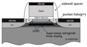
As we can see, the cross-section of these real transistors are very different from the idealized transistor in Fig. 1. A simplified cross-section of a submicron transistor is shown in Fig. 5. A few noteworthy characteristics of advanced MOSFETs:
- Gate Electrode
- Ultra-thin Gate Dielectrics
- Source/Drain Engineering
- Short-Channel Effects
- Retrograde Doping
- Pocket Implants
Process Variations
In addition to these advanced MOSFET characteristics, the presence of run-to-run parameter variations, either systematic or random, adds another layer of uncertainty to the design process. These variations must be taken into consideration when designing analog circuits. One option is to use Monte Carlo simulations similar to our activity on passive element variations. However, for transistors with hundreds of parameters, these simulations would take a significant amount of time and computing resources even for relatively simple circuits.
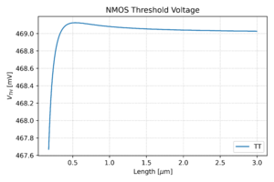
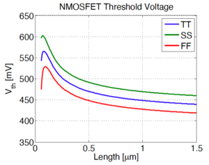
Corner analysis is an alternative to Monte Carlo simulation where the effects of individual device parameter variations are combined to determine device- or circuit-level performance variations. Worst-case and best-case performance variations are then identified as corners. For example, we can plot the speed of the NMOS and PMOS transistors as the threshold voltage, mobility, and oxide capacitance are varied. The worst cases, also known as the corner cases are shown in Fig. 6. These corners can then be translated back into the device parameter domain, e.g. the threshold voltage, to determine an acceptable range of values, depicted in Fig. 7.
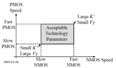 Figure 6: MOSFET speed corners[5]. |
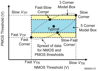 Figure 7: MOSFET threshold voltage corners[5]. |
Thus, instead of simulating random points, we can just simulate the device or circuit performance at these points to determine their corner behavior, e.g. the typical NMOS, typical PMOS case (TT corner), the fast NMOS, fast PMOS case (FF corner), the slow NMOS, slow PMOS case (SS corner), etc.
Short-Channel Effects
If our "simple" models are not sufficient, do we rely purely on simulators? No.
- Simulator models (e.g. BSIM) are not always based on real measurements
- Models inherently compromise accuracy for speed
We need to know the important short-channel effects so we know what to look for:
- The model might be wrong or might not include certain physical mechanisms
Threshold Voltage
As the MOSFET channel length continues to scale, the distance between source and drain regions decreases. Due to this reduced distance, current can start to flow outside the designated channel area, i.e. deeper into the substrate. Thus, the gate voltage has less control of these currents since these currents are further away from the gate oxide, potentially leading to larger leakage currents. One way to prevent these sub-channel currents is to add halo or pocket implants, as shown in Fig. 8.
However, these implants result in the reverse short-channel effect, where the threshold voltage decreases as the transistor length increases, as shown in Figs. 9 and 10. Note that at shorter channel lengths, the halo implants are closer together, increasing the effective doping in the channel, thus increasing the threshold voltage. As the channel length is increased, the halo implants are pulled apart, increasing the channel region unaffected by the halo doping. This results in a reduction in threshold voltage.
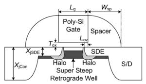 Figure 8: A cross-section of a bulk MOSFET showing the halo implants[6]. |
Drain Current
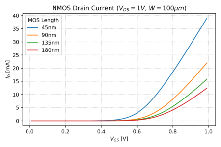
For relatively small electric fields, the drift velocity of an electron is given by . From this linear relationship between the drain electric field and drift velocity, we can derive the MOSFET square-law behavior. However, above a critical electric field, , the velocity starts to saturate, as seen in Fig. 11. Since , and for constant voltages, e.g. 1V, the electric field in deep sub-micron transistors can be very large. Thus, instead of a square law, to first order, we get a linear relationship between and . This can be seen in the graph in Fig. 12, for relatively large values of . The actual MOSFET behavior is actually somewhere between the square-law and the linear behavior, leading to the alpha-law MOSFET model:
-
(2)
-
Where . This is also due, in part, to the gate electric field acting on the carriers. In the square-law model, the gate field determines the amount of charge carriers in the channel, while the drain field determined the velocity of these charge carriers. However, as the transistor is scaled further, the gate field starts to accelerate the carriers towards the gate, degrading the mobility even more. This phenomenon is known as vertical field mobility degradation.
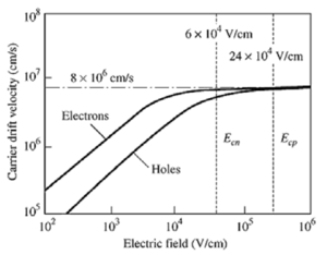 Figure 11: Velocity saturation[7]. |
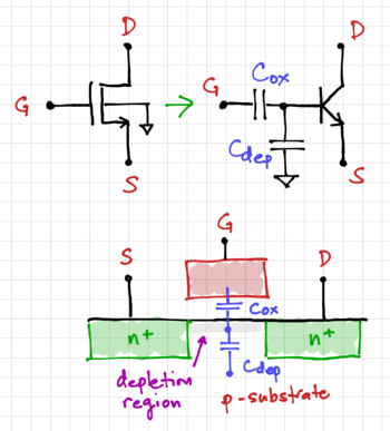
The square-law MOSFET model assumes that when . This is not true in real MOS transistors, since even if is not large enough to create a channel, diffusion current can flow, and the MOSFET behaves like a capacitively coupled BJT, as shown in Fig. 13.
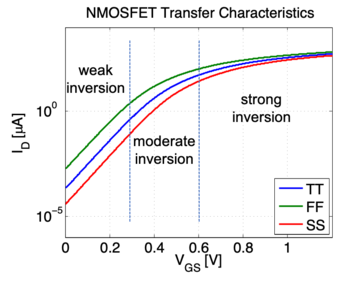
In this subthreshold region or the weak inversion region, the drain current is now a diffusion current instead of a drift current, and can be expressed as:
-
(3)
-
Where . The exponential nature of the drain current can be seen in Fig. 14. MOS transistors operating in the weak inversion region are considered "slow" since the drain current is relatively small, thus more time is needed to charge the necessary capacitances. However, the power consumption is also low, making operating in this region attractive for low-power applications. Note that due to the exponential nature of the current, variations in the threshold voltage will affect the drain current exponentially as well, making it more difficult to match devices.
In between the weak inversion region and the strong inversion region is the moderate inversion region, shown in Fig. 14, where the drain current has both drift and diffusion components. Operating MOS transistors in this region allows for relatively low-power operation, while maintaining some performance. However, this region is difficult to model, leading to a lack of closed-form expressions, or alternatively expressions that are interpolations between the strong and weak inversion regions.
Output Resistance
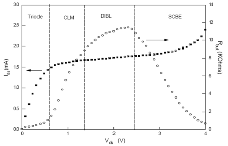
Aside from the MOSFET transfer characterisitics as captured by the vs. curves, we are also interested in its deep-submicron output characteristics, i.e. the behavior of the drain current as we vary the drain-to-source voltage, since this determines the output resistance:
-
(4)
-
In the square-law model, the drain current saturates to a value independent of as the channel pinches off. However, as we increase , the length of the pinch-off region also increases, reducing the effective channel length, thus increasing the current. This mechanism is called channel length modulation (CLM). We normally model this effect, using a CLM coefficient, , as:
-
(5)
-
The square-law model also assumes that the gate voltage is solely responsible for lowering the potential barrier between the source and the drain. However, as the channel length decreases, the potential barrier becomes thin enough that the drain voltage can also start lowering this potential barrier, effectively reducing the MOSFET threshold voltage. This drain-induced barrier lowering (DIBL) further increases the drain current as is increased.
As the transistor channel length is reduced, the drain-to-source electric field increases, leading to high-velocity carriers, or hot carriers. When these energetic carriers collide with the silicon lattice, they can dislodge electrons via impact ionization. This generates a substrate current, which once again results in an increase in total drain current. This mechanism is known as the substrate current body effect.
Thus, at low lateral fields, channel length modulation (CLM) dominates, while at medium electric fields, the dominant mechanism is the drain-induced barrier lowering (DIBL), and at very high electric fields, the substrate current body effect (SCBE) is the dominant, as seen in Fig.14.
References
- ↑ SPICE (Simulation Program with Integrated Circuit Emphasis) https://en.wikipedia.org/wiki/SPICE
- ↑ BSIM (Berkeley Short-channel IGFET Model) https://bsim.berkeley.edu/
- ↑ 3.0 3.1 3.2 M. T. Bohr and I. A. Young, CMOS Scaling Trends and Beyond, in IEEE Micro, vol. 37, no. 6, pp. 20-29, November/December 2017, doi: 10.1109/MM.2017.4241347. IEEExplore link
- ↑ Kim, Yong-bin, Challenges for Nanoscale MOSFETs and Emerging Nanoelectronics. Transactions on Electrical and Electronic Materials 11 (2010): 93-105. link
- ↑ 5.0 5.1 Phillip Allen's slides on MOSFET Large Signal Models.
- ↑ Jaffari, Javid & Anis, Mohab. (2008). Variability-Aware Bulk-MOS Device Design. Computer-Aided Design of Integrated Circuits and Systems, IEEE Transactions on. 27. 205 - 216. 10.1109/TCAD.2007.907234.
- ↑ 7.0 7.1 Elad Alon's slides on MOS models for design.
Further Reading
- M. T. Bohr and I. A. Young, CMOS Scaling Trends and Beyond, in IEEE Micro, vol. 37, no. 6, pp. 20-29, November/December 2017, doi: 10.1109/MM.2017.4241347. IEEExplore link
- Kim, Yong-bin, Challenges for Nanoscale MOSFETs and Emerging Nanoelectronics. Transactions on Electrical and Electronic Materials 11 (2010): 93-105. link
