Difference between revisions of "229-A1.2"
| Line 120: | Line 120: | ||
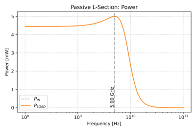
We can use this Python script to run ngspice, collect simulation data, and plot the results. Fig. 1 shows the power into the matching network, and the power delivered to the load. As expected, <math>P_{\mathrm{IN}}=P_{\mathrm{LOAD}}</math> since the ideal matching network is lossless, and the maximum is: | We can use this Python script to run ngspice, collect simulation data, and plot the results. Fig. 1 shows the power into the matching network, and the power delivered to the load. As expected, <math>P_{\mathrm{IN}}=P_{\mathrm{LOAD}}</math> since the ideal matching network is lossless, and the maximum is: | ||
| + | {{NumBlk|::|<math>P_{\mathrm{LOAD},\max} = P_{\mathrm{IN},\max} = \frac{1}{4}\frac{V_s^2}{R_S} = 5\mathm{mW}</math>|{{EquationRef|7}}}} | ||
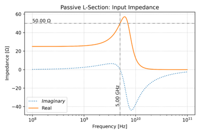
| + | Which is in agreement with our simulation results. Fig. 2 shows the input impedance of the matching network, and at 5GHz, the impedance is purely real, and is equal to the source impedance. | ||
{| | {| | ||
Revision as of 02:22, 7 September 2020
- Activity: Passive Matching Networks
- Instructions: Each activity is structured as a tutorial, and you are expected to download the netlists, run the simulation, and make sure you understand the concepts and ideas presented. Should you have any questions, clarifications, or issues, please contact your instructor as soon as possible.
- If you are new to ngspice, please visit the ngspice Tutorial page.
- At the end of this activity, the student should be able to:
- Design and verify the performance of passive impedance matching circuits using ngspice.
Contents
L-Section Matching Network Walk-Through
Let's design a single L-section circuit between a voltage source with output resistance, and an amplifier with input resistance, .
- Calculate the matching factor, ,and the quality factor, .
-
(1)
-
-
(2)
-
- Calculate the value of the reactance parallel to the larger resistance. In this case, the larger resistance is .
-
(3)
-
- Calculate the second reactance, , used to cancel .
-
(4)
-
- If we want a lowpass matching circuit, we need to use a capacitor for , and an inductor for . We can then calculate the capacitor and inductor values for .
-
(5)
-
-
(6)
-
Simulating the Matching Circuit
We can then create a SPICE netlist so we can verify the performance of our matching network. For circuits that you will reuse often, it is more often convenient to create a sub-circuit. In this case, a sub-circuit for our lowpass L-section, which we can save in a separate file, (such as matching_subckts.sp).
 1 * Passive Matching Circuits
 2 * LPA 05 Aug 2020
 3 .subckt l_match_lp hiR loR C=1p L=1n
 4
 5 V1		hiR z	dc=0 ac=0
 6 C1		z y 	{C}
 7 VC1		y 0	dc=0 ac=0
 8 L1		loR x	{L}
 9 VL1		x z	dc=0 ac=0
10
11 .ends l_match_lp
Note that the two voltage sources, VC1, VL1 and V1, do not affect the circuit since they are set to zero volts. These dummy voltage sources are just there so we can measure the currents in all the branches of the L-section.
We can then instantiate this sub-circuit, as instance X1, in our main SPICE file:
 1 * Passive Matching Circuits
 2 * LPA 05 Aug 2020
 3
 4 .options savecurrents seed=random
 5 .include matching_subckts.sp
 6
 7 X1 		hir lor		l_match_lp		C=636.62f L=795.77p
 8 Rs		hir vin		50
 9 Rl		lor 0		25
10
11 Vs		vin 0		dc=0 ac=1
12
13 .control
14
15 ac dec 1000 100meg 100G
16
17 let pin = abs(v(hir)*i(vs))
18 let pout = abs(v(lor)*i(v.x1.vl1))
19
20 let zin_imag = imag(v(hir)/(-i(vs)))
21 let zin_real = real(v(hir)/(-i(vs)))
22
23 let zout_imag = imag(v(lor)/(-i(v.x1.vl1)))
24 let zout_real = real(v(lor)/(-i(v.x1.vl1)))
25
26 meas ac poutmax max pout from=100meg to=100G
27
28 meas ac zin_real_f0 find zin_real at=5G
29 meas ac zin_imag_f0 find zin_imag at=5G
30
31 meas ac zout_real_f0 find zout_real at=5G
32 meas ac zout_imag_f0 find zout_imag at=5G
33
34 wrdata l_match_lp_a1.2.1.dat v(hir) (-i(vs)) v(lor) (-i(v.x1.vl1))
35
36 .endc
37
38 .end
We can also include simple expressions to calculate the power entering the matching network, the power delivered to , the input and output impedances, as well as the value of the maximum power delivered to the load, and the impedances at . We add the negative signs since in SPICE, positive current is the current flowing into the positive terminal of a voltage source.
Running the simulation via terminal would yield:
******
** ngspice-31 : Circuit level simulation program
** The U. C. Berkeley CAD Group
** Copyright 1985-1994, Regents of the University of California.
** Please get your ngspice manual from http://ngspice.sourceforge.net/docs.html
** Please file your bug-reports at http://ngspice.sourceforge.net/bugrep.html
******
ngspice 1 -> source matching.sp

Circuit: * passive matching circuits

Doing analysis at TEMP = 27.000000 and TNOM = 27.000000


No. of Data Rows : 3001
poutmax             =  5.000000e-03 at=  5.000345e+09
zin_real_f0         =  4.999970e+01
zin_imag_f0         =  -3.711545e-05
zout_real_f0        =  2.500000e+01
zout_imag_f0        =  -2.775922e-15
As expected, we get 3000 points since we are running the simulation over 3 decades (100MHz to 100GHz) at 1000 points per decade. We also get the results of our meas statements, with the maximum output power at 5mW, occurring at 5GHz. At this frequency, again, as expected, the input and output impedances are real, and they match the source and load resistances.
Plotting the Results
We can use this Python script to run ngspice, collect simulation data, and plot the results. Fig. 1 shows the power into the matching network, and the power delivered to the load. As expected, since the ideal matching network is lossless, and the maximum is:
-
(7)
-
Which is in agreement with our simulation results. Fig. 2 shows the input impedance of the matching network, and at 5GHz, the impedance is purely real, and is equal to the source impedance.
Design Problem 1:
In this section, you are asked to design a T-network to match a voltage source with source resistance to a load, with a required .


