Difference between revisions of "MOS Transistors"
| Line 41: | Line 41: | ||
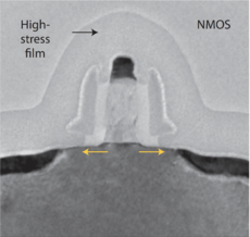
[[File:Intel 90nm nmos.png|thumb|230px|Figure 2: Intel 90nm MOSFET with tensile channel strain<ref name="Bohr2017">M. T. Bohr and I. A. Young, ''CMOS Scaling Trends and Beyond,'' in IEEE Micro, vol. 37, no. 6, pp. 20-29, November/December 2017, doi: 10.1109/MM.2017.4241347. [https://ieeexplore.ieee.org/document/8119702 IEEExplore link]</ref>.]] | [[File:Intel 90nm nmos.png|thumb|230px|Figure 2: Intel 90nm MOSFET with tensile channel strain<ref name="Bohr2017">M. T. Bohr and I. A. Young, ''CMOS Scaling Trends and Beyond,'' in IEEE Micro, vol. 37, no. 6, pp. 20-29, November/December 2017, doi: 10.1109/MM.2017.4241347. [https://ieeexplore.ieee.org/document/8119702 IEEExplore link]</ref>.]] | ||
| | | | ||
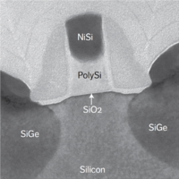
| − | [[File:Intel 65nm mosfet.png|thumb|200px|Figure 3: Intel 65nm MOSFET using <math>\mathrm{SiO_2}</math> as dielectric and polysilicon as the gate material<ref name="Bohr2017"/>.]] | + | [[File:Intel 65nm mosfet.png|thumb|200px|Figure 3: Intel 65nm MOSFET using <math>\mathrm{SiO_2}</math> as dielectric and [https://en.wikipedia.org/wiki/Polycrystalline_silicon polysilicon] as the gate material<ref name="Bohr2017"/>.]] |
| | | | ||
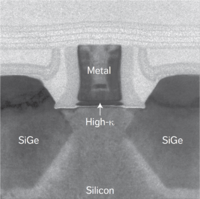
| − | [[File:Intel 45nm mosfet.png|thumb|200px|Figure 4: Intel 45nm MOSFET with metal gate and hafnium-based dielectric.<ref name="Bohr2017"/>.]] | + | [[File:Intel 45nm mosfet.png|thumb|200px|Figure 4: Intel 45nm MOSFET with metal gate and [https://en.wikipedia.org/wiki/Hafnium hafnium]-based dielectric.<ref name="Bohr2017"/>.]] |
|} | |} | ||
Revision as of 12:31, 17 August 2020
Analog circuits are generally sensitive to the nuances and details of transistor behavior, requiring precise and/or well-controlled voltages, currents, etc. Digital circuits, on the other hand, can have much larger margins of error due to their inherent noise margins and regenerative properties. Thus, we want to be able to model these nuances and details of transistor behavior in order to predict their effects on our circuits.
Contents
Transistor Models
Transistor models enable us to describe and predict the behavior of the circuits we build using these transistors by:
- Providing us with a window into the physical device characteristics (e.g. dimensions, material and device properties, etc.) and processes (e.g. drift/diffusion currents, tunneling, charge transfer, etc.), and
- Allowing us to perform easy to do "experiments" using simulators such as SPICE[1].
Levels of Abstraction
The complexity of transistor models can range from very simple models, such as modeling the transistor as a simple controlled switch, to very complex models such as BSIM[2] models with hundreds of parameters.
We choose a model based on the questions we want answered. For example:
- For predicting the digital (boolean) functionality of a static CMOS gate, we can simply model the transistor as a controlled switch.
- However, if we want to predict the performance of the CMOS gate, we might need to model the ON current of the transistor as a current source in series with a switch.
- For high-precision analog circuits, we might need a BSIM model to predict the noise performance, settling time, stability, etc.
Note that "questions" that are more complicated require more complex and mathematically intensive models. Thus, it is best to match the model complexity to the problem or question we want answered. Further note that different models can be used to answer different questions at different stages of the design process.
The Square-Law MOSFET Model
The widely known square-law MOSFET model is a good model for predicting the behavior of discrete and relatively large-sized transistors. It relates the drain saturation current to the gate-to-source voltage as:
-
(1)
-
Where is the electron mobility, is the gate-oxide capacitance per unit area, dependent on the permittivity and thickness of the gate oxide layer, and is the transistor threshold voltage.
However, the square-law model is inadequate for modeling short-channel behavior, since it is based on the following assumptions (not a complete list):
- The channel charge density is determined only by the vertical electric field due to .
- Drift velocity is set only by the lateral electric field due to .
- The mobility of electrons and holes are constant.
- There are no diffusion currents, and that when .
Submicron Transistors
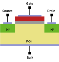
Due to manufacturing constraints and limitations, the structure of a deep submicron (with channel lengths of 65nm and below) transistors can differ quite dramatically from the idealized structure shown in Fig. 1. For an simple overview of the CMOS fabrication process, you can watch Silicon Run I (1996).
The cross section of modern MOSFETs with lengths of 90nm, 65nm, and 45nm are shown in Figs. 2, 3 and 4.
 Figure 2: Intel 90nm MOSFET with tensile channel strain[3]. |
As we can see, the cross-section of these real transistors are very different from the idealized transistor in Fig. 1.
References
- ↑ SPICE (Simulation Program with Integrated Circuit Emphasis) https://en.wikipedia.org/wiki/SPICE
- ↑ BSIM (Berkeley Short-channel IGFET Model) https://bsim.berkeley.edu/
- ↑ 3.0 3.1 3.2 M. T. Bohr and I. A. Young, CMOS Scaling Trends and Beyond, in IEEE Micro, vol. 37, no. 6, pp. 20-29, November/December 2017, doi: 10.1109/MM.2017.4241347. IEEExplore link
Further Reading
- M. T. Bohr and I. A. Young, CMOS Scaling Trends and Beyond, in IEEE Micro, vol. 37, no. 6, pp. 20-29, November/December 2017, doi: 10.1109/MM.2017.4241347. IEEExplore link


