Difference between revisions of "CoE 197U MOS Differential Pairs"
| Line 34: | Line 34: | ||
The large signal characteristics of the MOS differential pair analysis is started by setting up a KVL equation from <math>V_{I1}</math> to <math>V_{I2}</math> and relating it to currents <math>I_{D1}</math> and <math>I_{D1}</math>, under the restriction that <math>I_{D1}+I_{D2}=I_{T}</math>. The following equations are valid given that the two transistors are saturated. | The large signal characteristics of the MOS differential pair analysis is started by setting up a KVL equation from <math>V_{I1}</math> to <math>V_{I2}</math> and relating it to currents <math>I_{D1}</math> and <math>I_{D1}</math>, under the restriction that <math>I_{D1}+I_{D2}=I_{T}</math>. The following equations are valid given that the two transistors are saturated. | ||
| − | ::<math>I_{D1}=\frac{I_{T}}{2}+\frac{k'}{4}\frac{W}{L}V_{id}\sqrt{\frac{4I_T}{k'\frac{W}{L}}-V_{id}^2}</math> | + | ::For <math>|V_{id}|<V_{id,max}=\sqrt{\frac{2I_T}{k'\frac{W}{L}}}</math>: |
| − | ::<math>I_{D2}=\frac{I_{T}}{2}-\frac{k'}{4}\frac{W}{L}V_{id}\sqrt{\frac{4I_T}{k'\frac{W}{L}}-V_{id}^2}</math> | + | {{NumBlk|::|<math>I_{D1}=\frac{I_{T}}{2}+\frac{k'}{4}\frac{W}{L}V_{id}\sqrt{\frac{4I_T}{k'\frac{W}{L}}-V_{id}^2}</math>|{{EquationRef|1}}}} |
| + | {{NumBlk|::|<math>I_{D2}=\frac{I_{T}}{2}-\frac{k'}{4}\frac{W}{L}V_{id}\sqrt{\frac{4I_T}{k'\frac{W}{L}}-V_{id}^2}</math>|{{EquationRef|2}}}} | ||
| − | When <math>|V_{id}|> | + | When <math>|V_{id}|>V_{id,max}</math>, all of <math>I_T</math> will flow only through one transistor while the other transistor will be in cut-off. This is shown in Fig. 5. Thus, the tail current is effectively steered or distributed between M1 and M2 by <math>V_{id}</math>, regardless of the <math>V_{ic}</math> as long as the transistors are saturated and the current source is still operating as intended. |
{| | {| | ||
| Line 47: | Line 48: | ||
|} | |} | ||
| − | Assuming that the load is a pair of equal and matched resistors such in Fig. 6, the output voltage is determined by KVL and the difference in drain currents. | + | Assuming that the load is a pair of equal and matched resistors such in Fig. 6, the output voltage is determined by KVL (Eq. 3) and the difference in drain currents (Eqs. 1 and 2). The resulting expression is Eq. 4. The plot of this function is the middle portion of Fig. 7. |
| − | ::<math>V_{od}=V_{o1}-V_{o2}=(V_{CC}-I_{D1}R_D)-(V_{CC}-I_{D2}R_D)</math> | + | {{NumBlk|::|<math>V_{od}=V_{o1}-V_{o2}=(V_{CC}-I_{D1}R_D)-(V_{CC}-I_{D2}R_D)</math>|{{EquationRef|3}}}} |
| − | ::<math>V_{od}=-R_D\frac{k'}{2}\frac{W}{L}V_{id}\sqrt{\frac{4I_T}{k'\frac{W}{L}}-V_{id}^2}</math> | + | ::For <math>|V_{id}|<V_{id,max}</math>: |
| + | {{NumBlk|::|<math>V_{od}=-R_D\frac{k'}{2}\frac{W}{L}V_{id}\sqrt{\frac{4I_T}{k'\frac{W}{L}}-V_{id}^2}</math>|{{EquationRef|4}}}} | ||
| + | |||
| + | Beyond <math>|V_{id,max}|</math> the currents rail, and therefore, the differential output voltage also rail. Fig. 7 also shows that the amplifier has an inverting gain. | ||
== Small Signal AC and Half Circuit Analysis == | == Small Signal AC and Half Circuit Analysis == | ||
Revision as of 13:54, 15 April 2021
The differential pair is one of the most commonly used circuit blocks in analog IC design. It enables amplifiers to have not just two, but specifically, differential inputs and act based only or mostly on the difference of the input signals.
The main references for this topic are chapters 3.5 and 4.3.5 of the Analysis and Design of Analog Integrated Circuits book.
Contents
Fully Differential Amplifier Signal and Gain Definitions
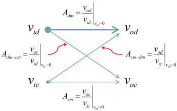
Before proceeding, the voltage signals to be dealt with need to be defined first to aid in the discussion. We will look at a general fully differential amplifier with a differential input and a differential output. The differential input/output voltages are the difference of input/output voltages. The common-mode input/output voltages are the average of the input/output voltages. Given how , , , and are related (Fig. 1), knowledge of any two can be used to infer the remaining two.
The presence of differential and common-mode inputs and outputs require a clarification on how the gains are defined (Fig. 2). An ideal fully differential amplifier will have a very large and very low , as the arrows' thickness suggests. and are also ideally very low. and are both zero if the circuit is perfectly balanced, which requires that components are perfectly matched in terms of device properties and bias.
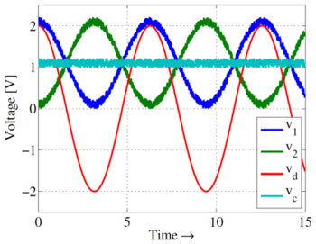
The advantage of having a differential input is the ability to reject signals that are common to both inputs such as noise that is coupled to both input signals. As can be seen in Fig. 3, the noise present on both inputs, and , does not appear at the differential signal . If indeed the differential pair works only on this differential input signal, then the noise will not be amplified with the actual input information. The same property also allows the circuit to be less sensitive to the DC offset of the two signals. This makes differential amplifiers easy to cascade without the need for AC-coupling capacitors, which generally need to be large and are costly in IC implementations. However, care is still needed when dealing with large signal swings and/or small supply voltages.
DC and Large Signal Analysis
The MOS differential pair or the source-coupled pair is shown in Figs. 4a and 4b. In source-coupled pairs, the source nodes are tied together. The current source is referred to as the tail current source. A simple but crude way of providing current to the differential pair is by using a tail resistor instead of a current source.
Assume that the transistors are perfectly matched/identical. Assume also that anything connected above the drain terminals are perfectly balanced or symmetric. For the DC analysis, assume that for simplicity to highlight the basic operation of the circuit.
Consider the differential pair with a tail current source (Fig. 4a). When there is no differential input, then the input voltages and must exactly be equal at some common-mode voltage . By virtue of symmetry, the transistors must have the same current, i.e. . Such is the case without even taking note of what is the actual . If should change, adjusts to maintain the Vgs that corresponds to . Since can be inferred from the transistor dimensions and the DC current, which are both constant, then is maintained even if changes, again, under the assumption that or is very large.
The large signal characteristics of the MOS differential pair analysis is started by setting up a KVL equation from to and relating it to currents and , under the restriction that . The following equations are valid given that the two transistors are saturated.
- For :
-
(1)
-
-
(2)
-
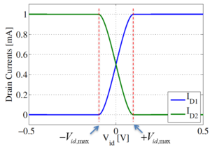
When , all of will flow only through one transistor while the other transistor will be in cut-off. This is shown in Fig. 5. Thus, the tail current is effectively steered or distributed between M1 and M2 by , regardless of the as long as the transistors are saturated and the current source is still operating as intended.
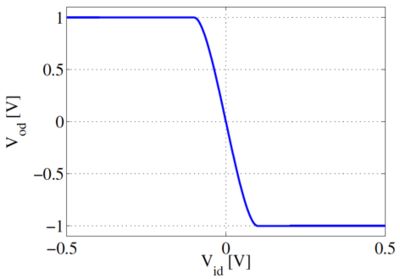
Assuming that the load is a pair of equal and matched resistors such in Fig. 6, the output voltage is determined by KVL (Eq. 3) and the difference in drain currents (Eqs. 1 and 2). The resulting expression is Eq. 4. The plot of this function is the middle portion of Fig. 7.
-
(3)
-
- For :
-
(4)
-
Beyond the currents rail, and therefore, the differential output voltage also rail. Fig. 7 also shows that the amplifier has an inverting gain.


