CoE 197U MOS Differential Pairs
The differential pair is one of the most commonly used circuit blocks in analog IC design. It enables amplifiers to have not just two, but specifically, differential inputs and act based only or mostly on the difference of the input signals.
The main references for this topic are chapters 3.5 and 4.3.5 of the Analysis and Design of Analog Integrated Circuits book[1].
Contents
Fully Differential Amplifier Signal and Gain Definitions
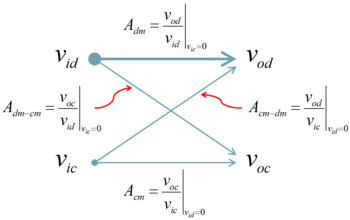
Before proceeding, the voltage signals to be dealt with need to be defined first to aid in the discussion. We will look at a general fully differential amplifier with a differential input and a differential output. The differential input/output voltages are the difference of input/output voltages. The common-mode input/output voltages are the average of the input/output voltages. Given how , , , and are related (Fig. 1), knowledge of any two can be used to infer the remaining two.
The presence of differential and common-mode inputs and outputs require a clarification on how the gains are defined (Fig. 2). An ideal fully differential amplifier will have a very large and very low , as the arrows' thickness suggests. and are also ideally very low. and are both zero if the circuit is perfectly balanced, which requires that components are perfectly matched in terms of device properties and bias.
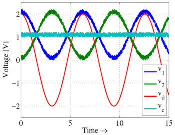
The advantage of having a differential input is the ability to reject signals that are common to both inputs such as noise that is coupled to both input signals. As can be seen in Fig. 3, the noise present on both inputs, and , does not appear at the differential signal . If indeed the differential pair works only on this differential input signal, then the noise will not be amplified with the actual input information. The same property also allows the circuit to be less sensitive to the DC offset of the two signals. This makes differential amplifiers easy to cascade without the need for AC-coupling capacitors, which generally need to be large and are costly in IC implementations. However, care is still needed when dealing with large signal swings and/or small supply voltages.
DC and Large Signal Analysis
The MOS differential pair or the source-coupled pair is shown in Figs. 4a and 4b. In source-coupled pairs, the source nodes are tied together. The current source is referred to as the tail current source. A simple but crude way of providing current to the differential pair is by using a tail resistor instead of a current source.
Assume that the transistors are perfectly matched/identical. Assume also that anything connected above the drain terminals are perfectly balanced or symmetric. For the DC analysis, assume that for simplicity to highlight the basic operation of the circuit.
Consider the differential pair with a tail current source (Fig. 4a). When there is no differential input, then the input voltages and must exactly be equal at some common-mode voltage . By virtue of symmetry, the transistors must have the same current, i.e. . Such is the case without even taking note of what is the actual . If should change, adjusts to maintain the Vgs that corresponds to . Since can be inferred from the transistor dimensions and the DC current, which are both constant, then is maintained even if changes, again, under the assumption that or is very large.
The large signal characteristics of the MOS differential pair analysis is started by setting up a KVL equation from to and relating it to currents and , under the restriction that . The following equations are valid given that the two transistors are saturated.
- Disregarding ,
- For :
-
(1)
-
-
(2)
-
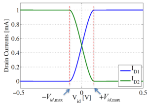
When , all of will flow only through one transistor while the other transistor will be in cut-off. This is shown in Fig. 5. Thus, the tail current is effectively steered or distributed between M1 and M2 by , regardless of the as long as the transistors are saturated and the current source is still operating as intended.
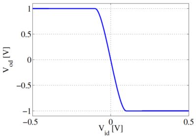
Assuming that the load is a pair of equal and matched resistors such in Fig. 6, the output voltage is determined by KVL (Eq. 3) and the difference in drain currents (Eqs. 1 and 2). The resulting expression is Eq. 4. The plot of this function is the middle portion of Fig. 7.
-
(3)
-
- For :
-
(4)
-
Beyond the currents rail, and therefore, the differential output voltage also rail. Fig. 7 also shows that the amplifier has an inverting gain.
can also be rewritten as . Thus, designing the differential pair with a larger increases the differential input voltage range at which both transistors are saturated. However, it will be shown on later in this module that a larger overdrive voltage of the differential pair leads to poorer gain, CMRR, and sensitivity to mismatch.
Small-Signal AC and Half Circuit Analysis
Taking the limit as , it can be shown that the approaches a linear function, and the small-signal gain is which must be very familiar. Note that this is evaluated at the case where is around 0, where , and that the small-signal gain represents the slope of the vs. plot for very small . The expression is not very accurate because Eqs. 4 and 5 assumes that is very large.
-
(5)
-
Eq. 5 shows that the small-signal differential gain is dependent only on , the transistor dimensions, and the tail current. Changing the DC bias of the input voltage will not affect the gain, as long as the transistors are saturated and the tail current is fixed.
Analyzing the circuit’s small-signal model will help determine the small-signal gains easier, without having to assume that . The full small-signal equivalent circuit is shown in Fig. 8. Here we are assuming that the tail current source is non-ideal and has some finite small-signal resistance . Note also, that transistors’ are maintained.
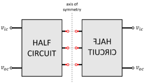
The differential gain is analyzed with . If the circuit is perfectly balanced, it follows that . Due to symmetry, analyzing only half of the circuit should already give us enough information. With differential inputs only in play, one side/half can be considered “positive” while the other side/half can be considered “negative.” Thus, the middle point/s of the differential circuit must be at small-signal 0V. We can divide the circuit in half and place a virtual differential ground at each wire that is cut by the axis of symmetry. Note, however, that we must still maintain the voltage definitions with (i.e. remains , etc.) as in Fig. 9.
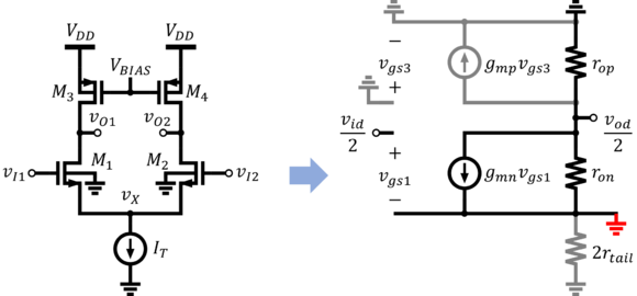
Taking the left-side of Fig. 8 for the differential half circuit analysis, we end up with Fig. 10. Note that the voltages are still and . The tail resistance was also divided into two ’s to properly cut the circuit in half. The source is at (differential) ground, and thus, is effectively shorted. The remaining portion of the half circuit resembles that of a resistor-loaded common source, whose gain is . However, the input is while the output is . Thus, this gain is given by:
-
(6)
-
For the common-mode case, must be set to zero which consequently makes . This time, since we are applying common or the same excitation on both sides of a balanced circuit then, there must be no current flowing either from left to right or from right to left since the two sides are at the same potential. Thus, portions that are cut in dividing the circuit into two are left open, instead of placing a ground, as shown in Fig. 11. The common-mode half circuit is shown in Fig. 12. This circuit follows the same structure as a common source amplifier with emitter degeneration, and with and . The gain of such a circuit is approximately . Thus, the common-mode gain is given by Eq. 7. Note that if the current source were ideal, then and .
-
(7)
-
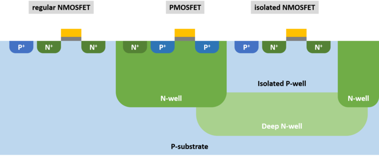
Note that the previous expression is valid only when there is no body effect. However, this is not true for the circuit in Fig. 6 since the body is grounded while the source is not. In a standard CMOS technology with a p-type substrate, shorting the PMOS source to its body is easy since each PMOS has its own n-well. However, for NMOS, the body is also the substrate that is shared across the whole chip. It will only be possible to short the NMOS source to the body, without shorting the rest of the substrate, if the technology has a way to isolate and tap an NMOS’s p-type body from the rest of the chip. Such a feat is possible with a triple well technology (Fig. 13).
If the body is not or cannot be tied to the source, then the body effect occurs, where changes in cause threshold voltage to change. Thus, when the source potential changes, the drain current changes not only because changes but also because the threshold voltage changes. The small-signal common-mode half circuit with the body effect is shown in Fig. 14. Analysis of this half circuit will lead to a common-mode gain expressed by Eq. 8. Note that the body transconductance is given by
-
(8)
-
Note that there is no body effect in the differential circuit even if the source not shorted to the body since the bulk is grounded and the source is at the differential ground. Thus, the small-signal is 0.
CMRR
-
(9)
-
The common-mode rejection ratio or CMRR is given by Eq. 9. CMRR is a primary figure of merit for differential amplifiers. The higher the CMRR, the better. For the differential pair with body effect, the CMRR is approximately given by Eq. 10. The CMRR of the differential amplifier improves with increasing and is independent of the load resistance. The equation also shows that the body effect helps improve CMRR since χ is a positive quantity typically around 0.1 to 0.3. Although the body-effect improves CMRR by reducing Acm, it must be noted that the body effect still influences the threshold voltage and can impact the allowable DC voltage levels and signal swing.
-
(10)
-
Eq. 10 can be expressed in terms of the transistor currents and overdrive voltage. Assuming that the tail current source is some NMOS transistor biased at saturation, then the tail resistance must be some , and the expressions below can be obtained. The equations show that to improve CMRR, the length of the tail current source transistor must be increased (to decrease ) while the overdrive of the differential pair must be decreased (larger width-length ratio for the same current).
Differential Pair with Active Load
Larger gains can be achieved when using active loads. Fig. 15 shows an active-loaded differential pair. The two load transistors act like current sources. M3 and M4 must be biased such that at DC.
At AC, the gates of M3 and M4 are grounded since is some constant voltage bias or reference. Aside from that, the gates of M3 and M4 are at differential ground. Thus, at AC, , M3 and M4 simply present a resistance , and the differential gain must be
-
(11)
-
Although the gain of this circuit is larger compared to the resistor-loaded case, maintaining the correct DC operation is harder. Note that the output DC voltage is not well-defined unlike in the resistor-loaded case where can be easily found to be . Even a minor mismatch between , , and will cause the output nodes to rail up or down, putting the load transistors or the differential pair in the linear region, respectively. Thus, some form of common-mode feedback or CMFB is necessary to ensure that the active-loaded differential pair will have a stable DC output level and to ensure that transistors are saturated. CMFB is discussed in Chapter 12.4 of the book (optional, for further reading).
Differential to Single-Ended Output Conversion
A lot of applications require a single-ended output. However, the differential pair’s output is differential by default. Taking the output from one side will cut the transconductance in half, and thus, the gain in half. This is not an ideal scenario since we are paying with current and power to increase but benefitting only from half of it. A better way to convert from a differential to a single-ended output is using a current mirror load (Fig. 16).
DC Analysis
The mirroring action happens in both DC and AC. At DC, the current will be mirrored to . If the transistors are perfectly matched and , then . Note that this circuit does not require a separate biasing circuit since the diode-connected M3 automatically generates the necessary gate voltage. Also, if the transistors are perfectly matched and if indeed the currents through M3 and M4 are the same, then, must be at the same potential as the drain of M3.
Small-Signal AC Analysis
The small-signal model of the current mirror-loaded differential pair is also shown in Fig. 16. Because the load is not anymore balanced (M3 is diode-connected while M4 is not), then, half circuit analysis cannot be used. The tail current source is not anymore grounded, as there is no true differential ground in this circuit. The gain can be determined from the and of the circuit and using .
Transconductance
For , the output is grounded and the output current , as stimulated from , is measured (Fig. 17). Note that simplifying assumptions are used to come up with easy-to-interpret results. First, the tail current source is assumed to be ideal (i.e. ). Also, and are assumed to be very large, that they will not have a significant effect to the overall .
The diode-connected M3 can be modeled as a resistor with a value if . Note also that is shorted to ground at both sides and will not contribute any current to . The current can then be related to as follows. Thus, in this case, the load will mirror the AC current perfectly if , the transistors are perfectly matched, and which leads to .
Assume that is finite and that some current flows down from to ground. The equations below show that if the differential pair 's are very large, then the voltage is at 0V at small-signal. If the differential pair has equal currents at DC, then and . Interestingly, the assumption led to a conclusion that a differential ground approximately exists at the coupled source node. Note however that cannot be assumed when analyzing the circuit's output resistance because is expected to depend heavily on the transistors' .
- disregarding 's
There is another reason why a differential ground approximately exists at the coupled source node in the circuit in Fig. 17, even with finite . Note that the drain of M2 is shorted to ground while the drain of M1 is connected to a relatively small resistance, . If the resistance presented by M3 is small enough, then the drain of M1 is approximately at ground potential as well. Thus, the circuit operates in a nearly balanced behavior, and a differential ground appears at . However, this observation is true only for the circuit in Fig. 17. The nearly balanced behavior does not occur anymore when analyzing the circuit's output resistance or voltage gain because in these cases, the output node is not anymore grounded.
Combining the fact that and that is normally very large, then must be very small and the tail resistance can be effectively treated as open circuit. This also means that
- .
Since , then . It can be shown in a similar fashion that .
The currents , , and can therefore be related as follows, where is used to denote and .
The output current can finally be related to by:
-
(12)
-
Output Resistance
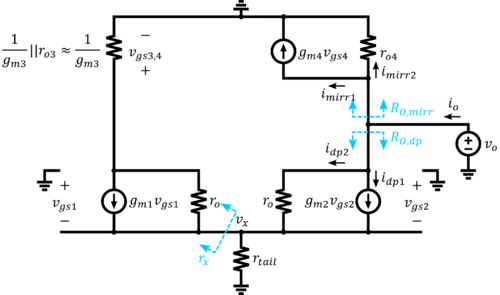
For the output resistance analysis, the transistor ’s are retained as shown in Fig. 18. A test voltage is connected at the output and the drawn output current is measured while the input is grounded. is still assumed such that M3 is still modeled as some resistor. The output current branches into 4 components: , , , and . The output resistance can be considered to have two components such that
- where and
The easiest to determine is which is just the current across the resistance .
The resistance presented by M1 and M3, as seen from the source of M2, can be lumped as some . This is in parallel with . The resistance can then be taken by analyzing M2 as an emitter degenerated transistor with an emitter resistance of . An emitter degenerated transistor has the output resistance . Thus,
The resistance (composed of M1 and M3) is obtained by analyzing the circuit in Fig. 19. The circuit can be seen as a source follower with some drain resistance. Refering to the original circuit of concern is The complete expression is shown below although is approximately , if .
An of is normally very small compared to . Thus, , and the resistance presented by the differential pair is given below. Similarly, it is assumed that .
Since , by current division, most of the current will flow through . Thus, the current through the resistance is almost the whole of and will be mirrored through M4.
The output resistance of the current mirror, from the component currents and is
Finally, the overall output resistance is the parallel combination of and .
-
(13)
-
Following the discussion presented and assumptions used, the differential pair presents a resistance of (and not simply ) at the output terminal, while the current mirror presents a resistance of (and not simply ).
In DC biased current mirrors, the output resistance will simply be the of the output transistor. However, in this circuit, some AC current is being mirrored as well, so the output resistance is more complicated.
Gain
The gain of the current mirror-loaded differential pair with the assumptions discussed is given below. The gain is non-inverting since the output is taken on the side of the negative input terminal.
-
(14)
-
Although the gain expression turns out to be very simple, it is important to understand the analysis and assumptions done along the way. This should provide some background on what happens or what changes when some of the assumptions cannot be done anymore. The concepts discussed should also help when analyzing the circuit from a different perspective (e.g. analyzing with noise or parasitics) or analyzing a similar circuit (e.g. with cascoded differential pairs and/or cascoded current mirror loads).
References
- ↑ Gray, Hurst, Lewis, Meyer, Analysis & Design of Analog Integrated Circuits, Wiley 2001.


