Difference between revisions of "CoE 197U MOS Differential Pairs"
(Created page with "The differential pair is one of the most commonly used circuit blocks in analog IC design. It enables amplifiers to have not just two, but specifically, differential inputs an...") |
|||
| Line 4: | Line 4: | ||
== Fully Differential Amplifier Signal and Gain Definitions == | == Fully Differential Amplifier Signal and Gain Definitions == | ||
| + | |||
| + | Before proceeding, the voltage signals to be dealt with need to be defined first to aid in the discussion. We will look at a general fully differential amplifier with a differential input and a differential output. The differential input/output voltages are the difference of input/output voltages. The common-mode input/output voltages are the average of the input/output voltages. Given how <math>v_1</math>, <math>v_2</math>, <math>v_d</math>, and <math>v_d</math> are related (Fig. 1), knowledge of any two can be used to infer the remaining two. | ||
| + | {| | ||
| + | | | ||
| + | [[File:Fully Differential Amplifier Voltage Definitions.png|thumb|450px|Fig. 1Fully Differential Amplifier Voltage Definitions]] | ||
| + | | | ||
| + | [[File:Fully Differential Amplifier Voltage Gain Definitions.png|thumb|350px|Fig. 2 Fully Differential Amplifier Voltage Gain Definitions]] | ||
| + | | | ||
| + | [[File:Cancellation of Common-mode Noise in Differential Signal.png|thumb|350px|Fig. 3 Cancellation of Common-mode Noise in Differential Signal]] | ||
| + | |} | ||
| + | |||
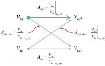
| + | The presence of differential and common-mode inputs and outputs require a clarification on how the gains are defined (Fig. 2). An ideal fully differential amplifier will have a very large <math>A_{dm}</math> and very low <math>A_{cm}</math>, as the arrows' thickness suggests. <math>A_{cm-dm}</math> and <math>A_{dm-cm}</math> are also ideally very low. <math>A_{cm-dm}</math> and <math>A_{dm-cm}</math> are both zero if the circuit is perfectly balanced, which requires that components are perfectly matched in terms of device properties and bias. | ||
| + | |||
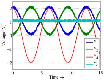
| + | The advantage of having a differential input is the ability to reject signals that are common to both inputs such as noise that is coupled to both input signals. As can be seen in Fig. 3, the noise present on both inputs, <math>v_{1}</math> and <math>v_{2}</math>, does not appear at the differential signal <math>v_{d}</math>. If indeed the differential pair works only on this differential input signal, then the noise will not be amplified with the actual input information. The same property also allows the circuit to be less sensitive to the DC offset of the two signals. This makes differential amplifiers easy to cascade without the need for AC-coupling capacitors, which generally need to be large and are costly in IC implementations. However, care is still needed when dealing with large signal swings and/or small supply voltages. | ||
| + | |||
== DC and Large Signal Analysis == | == DC and Large Signal Analysis == | ||
== Small Signal AC and Half Circuit Analysis == | == Small Signal AC and Half Circuit Analysis == | ||
Revision as of 11:11, 15 April 2021
The differential pair is one of the most commonly used circuit blocks in analog IC design. It enables amplifiers to have not just two, but specifically, differential inputs and act based only or mostly on the difference of the input signals.
The main references for this topic are chapters 3.5 and 4.3.5 of the Analysis and Design of Analog Integrated Circuits book.
Contents
Fully Differential Amplifier Signal and Gain Definitions
Before proceeding, the voltage signals to be dealt with need to be defined first to aid in the discussion. We will look at a general fully differential amplifier with a differential input and a differential output. The differential input/output voltages are the difference of input/output voltages. The common-mode input/output voltages are the average of the input/output voltages. Given how , , , and are related (Fig. 1), knowledge of any two can be used to infer the remaining two.
The presence of differential and common-mode inputs and outputs require a clarification on how the gains are defined (Fig. 2). An ideal fully differential amplifier will have a very large and very low , as the arrows' thickness suggests. and are also ideally very low. and are both zero if the circuit is perfectly balanced, which requires that components are perfectly matched in terms of device properties and bias.
The advantage of having a differential input is the ability to reject signals that are common to both inputs such as noise that is coupled to both input signals. As can be seen in Fig. 3, the noise present on both inputs, and , does not appear at the differential signal . If indeed the differential pair works only on this differential input signal, then the noise will not be amplified with the actual input information. The same property also allows the circuit to be less sensitive to the DC offset of the two signals. This makes differential amplifiers easy to cascade without the need for AC-coupling capacitors, which generally need to be large and are costly in IC implementations. However, care is still needed when dealing with large signal swings and/or small supply voltages.


