Difference between revisions of "CoE 197U The CMOS Inverter"
| Line 72: | Line 72: | ||
Where <math>V_{IL}</math> is the highest input voltage the inverter will still consider as a low voltage. Anything above this places the inverter in the high-gain region of the VTC, making it sensitive to noise and interference. Similarly, <math>V_{IH}</math> is the lowest input voltage the inverter will still consider as a high voltage. | Where <math>V_{IL}</math> is the highest input voltage the inverter will still consider as a low voltage. Anything above this places the inverter in the high-gain region of the VTC, making it sensitive to noise and interference. Similarly, <math>V_{IH}</math> is the lowest input voltage the inverter will still consider as a high voltage. | ||
| − | |||
| − | |||
== Noise in Digital Circuits == | == Noise in Digital Circuits == | ||
| − | + | One of the main advantages of digital circuits over analog circuits is its relatively good noise immunity. In a binary digital logic system, we reduce the amount of information carried by a digital signal to just 1 bit. This then increases the digital circuit's resiliency to interference noise from nearby signals, or from inherent device noise. The zero-gain regions of the ideal inverter VTC are ideal at the points near <math>V_H</math> and <math>V_L</math> since any disturbance nor noise added to the input voltage would just be ignored by the inverter, i.e. the output voltage will not change. | |
| − | |||
=== Noise Margins === | === Noise Margins === | ||
| + | To quantify this robustness to noise and interference, we define the following metrics: | ||
| + | * <math>NM_H = V_{OH}-V_{IH}</math> is the noise margin at the high output level, and is the maximum noise that can degrade the input high or logic '''1''' level to the point where the inverter might not recognize it as a high level anymore. | ||
| + | * <math>NM_L = V_{IL}-V_{OL}</math> is the noise margin at the low output level, and is the maximum noise that can degrade the input low or logic '''0''' level to the point where the inverter might not recognize it as a low level anymore. | ||
=== The Regenerative Property of Inverters === | === The Regenerative Property of Inverters === | ||
Revision as of 16:14, 10 March 2021
To understand the analysis and design of digital circuits, we will look at its fundamental element -- the digital gate. We will start with the simplest digital gate, the inverter.
Contents
The Inverter Voltage Transfer Characteristics (VTC)
The functionality of the inverter can be captured by looking at the output voltage as we change the input voltage, or the voltage-transfer characteristic (VTC).
The Ideal Inverter VTC
Let us define an ideal inverter, where:
-
(1)
-
Where is logic 1 voltage level, and in general may or may not be equal to the positive supply voltage, , and is logic 0 voltage level, and in general may or may not be equal to the negative supply voltage, . The VTC of this ideal inverter, as well as the standard inverter circuit symbol, is shown in Fig. 1.
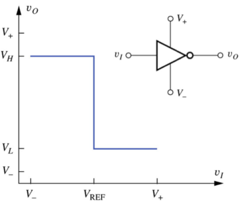 Figure 1: The ideal inverter voltage transfer characteristic (VTC)[1]. |
Inverter Implementations
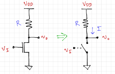
One implementation of the inverter is to use a single NMOS transistor and a resistor, as shown in Fig. 2. Using our switch model for the NMOS transistor, we can see that when the input is low or at logic 0, the output is pulled up to since the switch is open. When the input voltage is equal to , the switch is closed and the output is pulled down close to ground. For a finite on switch resistance, , the output voltage becomes:
-
(2)
-
Note that a finite will degrade (increase) low output voltage or logic 0 level. Additionally, the when the output of the NMOS inverter is low, there is a non-zero current flowing through the resistor, resulting in static power consumption, or power consumed from the supply even when there is no switching activity present in the circuit.
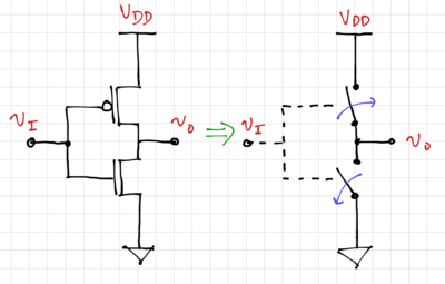
Another implementation of the inverter is to use an NMOS and a PMOS transistor. This complementary (CMOS) configuration turns on only one switch at a time since the gates of the two transistors are connected to each other. Thus, an input voltage of will turn on (close) the NMOS switch, and turn off (open) the PMOS switch since the gate-to-source voltage of the PMOS transistor is zero, pulling the inverter output down to ground. When the input voltage is ground or logic 0, the NMOS switch is open and the PMOS is closed, pulling the output up to .
Note that due to the complementary function of the CMOS inverter, there is no static current flowing when the output is either at logic 0 or logic 1. However, current will flow during the transition from 01 or 10.
We can derive the VTC of any inverter by determining the regions of operation of each transistor as we vary the input voltage. Fig. 4 shows the VTC of the CMOS inverter with the corresponding regions of operation, which are dependent on the input and output voltages. Note that:
- .
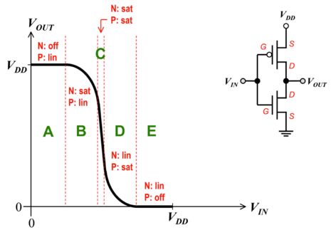 Figure 4: The CMOS inverter voltage transfer characteristic (VTC)[2]. |
Static Design Metrics
The general form of the inverter voltage transfer characteristic is shown in Fig. 5. We can define several metrics to enable us to determine how close the real VTC is to the ideal VTC.
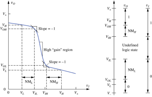 Figure 5: The non-ideal inverter voltage transfer characteristic (VTC)[1]. |
Consider the cascaded inverter in Fig. 6:
- is the output high or logic 1 output of the inverter, and is seen at the output when or logic 0 is placed at the input of the inverter.
- is the output low or logic 0 output of the inverter, and is seen at the output when or logic 1 is placed at the input of the inverter.
In the ideal inverter VTC in Fig. 1, we see that we have two flat regions (zero gain) and a vertical region (infinite gain). However, in a non-ideal VTC, the zero gain regions degrade into low gain regions where the absolute value of the slope is typically less than 1, and a high-gain region where the absolute value of the slope is greater than 1. The boundaries between the high- and low-gain regions are marked by the points where the absolute value of the slope of the VTC is equal to 1.
The two points with a slope of are shown in Fig. 5 and are located at the following coordinates:
- ()
- ()
Where is the highest input voltage the inverter will still consider as a low voltage. Anything above this places the inverter in the high-gain region of the VTC, making it sensitive to noise and interference. Similarly, is the lowest input voltage the inverter will still consider as a high voltage.
Noise in Digital Circuits
One of the main advantages of digital circuits over analog circuits is its relatively good noise immunity. In a binary digital logic system, we reduce the amount of information carried by a digital signal to just 1 bit. This then increases the digital circuit's resiliency to interference noise from nearby signals, or from inherent device noise. The zero-gain regions of the ideal inverter VTC are ideal at the points near and since any disturbance nor noise added to the input voltage would just be ignored by the inverter, i.e. the output voltage will not change.
Noise Margins
To quantify this robustness to noise and interference, we define the following metrics:
- is the noise margin at the high output level, and is the maximum noise that can degrade the input high or logic 1 level to the point where the inverter might not recognize it as a high level anymore.
- is the noise margin at the low output level, and is the maximum noise that can degrade the input low or logic 0 level to the point where the inverter might not recognize it as a low level anymore.
The Regenerative Property of Inverters
Inverter Delay
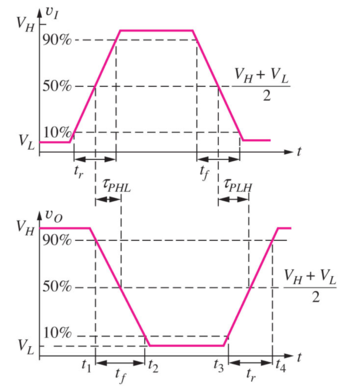 Figure: Logic delay definitions [1]. |
Power Dissipation
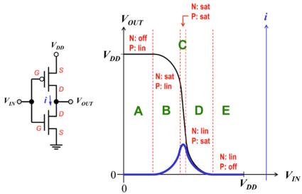 Figure : The CMOS switching current[3]. |
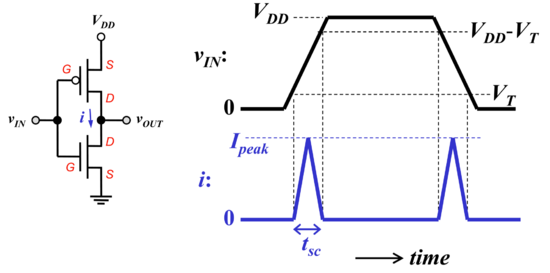 Figure : The CMOS transient power dissipation[3]. |


