Difference between revisions of "CMOS Technology and Fabrication"
| Line 15: | Line 15: | ||
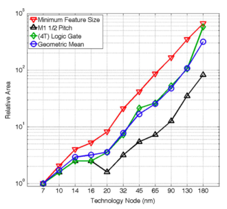
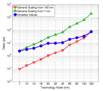
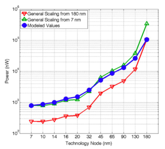
However, most advances in CMOS fabrication processes are, most of the time, driven by the performance requirements of digital circuits. As we can see in Figs. 1-3, scaling offers significant improvement in device area, speed, and power consumption. | However, most advances in CMOS fabrication processes are, most of the time, driven by the performance requirements of digital circuits. As we can see in Figs. 1-3, scaling offers significant improvement in device area, speed, and power consumption. | ||
{| | {| | ||
| − | | [[File:Stillmaker2017 area scaling.png|thumb| | + | | [[File:Stillmaker2017 area scaling.png|thumb|330px|Figure 1: Area improvement<ref name="stillmaker2017">Aaron Stillmaker, Bevan Baas, '''Scaling equations for the accurate prediction of CMOS device performance from 180nm to 7nm''', ''Integration'', Volume 58, 2017, Pages 74-81, ISSN 0167-9260, https://doi.org/10.1016/j.vlsi.2017.02.002.</ref>.]] |
| − | | [[File:Stillmaker2017 delay scaling.png|thumb| | + | | [[File:Stillmaker2017 delay scaling.png|thumb|330px|Figure 2: Delay improvement<ref name="stillmaker2017"/>.]] |
| − | | [[File:Stillmaker2017 power scaling.png|thumb| | + | | [[File:Stillmaker2017 power scaling.png|thumb|330px|Figure 3: Power consumption<ref name="stillmaker2017"/>.]] |
|- | |- | ||
|} | |} | ||
| + | |||
| + | In many cases, this reduction in delay, which translates to increased clock frequencies, it not really realized, due to the increased heat dissipation requirements at high clock frequencies. | ||
In order to take advantage of these new processes, analog designers have been forced to be more creative and innovative. | In order to take advantage of these new processes, analog designers have been forced to be more creative and innovative. | ||
Revision as of 17:08, 12 September 2020
Welcome to EE 220!
Since we are offering this class remotely, there will be many changes to our normal course delivery:
- There will be no face-to-face lecture classes. All the material will be made available via this site.
- There will be more emphasis on student-centric activities, e.g. analysis, design, and simulations. Thus, you will be mostly "learning by doing". In this context, we will set aside an hour every week for consultations and questions via video-conferencing.
- Grades will be based on the submitted deliverables from the activities. Though we will not be very strict regarding the deadlines, it is a good idea to keep up with the class schedule and avoid cramming later in the semester.
Let's get started!
CMOS Technology Review
Knowing how integrated devices are fabricated, and how the fabrication process affects the characteristics and performance of these devices, is one of the pillars of good analog circuit design. In analog design, we are interested in the relationships between the fabrication process steps and parameters to the device characteristics and performance.
However, most advances in CMOS fabrication processes are, most of the time, driven by the performance requirements of digital circuits. As we can see in Figs. 1-3, scaling offers significant improvement in device area, speed, and power consumption.
 Figure 1: Area improvement[1]. |
 Figure 2: Delay improvement[1]. |
 Figure 3: Power consumption[1]. |
In many cases, this reduction in delay, which translates to increased clock frequencies, it not really realized, due to the increased heat dissipation requirements at high clock frequencies.
In order to take advantage of these new processes, analog designers have been forced to be more creative and innovative.
Sources
- Phillip Allen's slides on CMOS fabrication.
References
- ↑ 1.0 1.1 1.2 Aaron Stillmaker, Bevan Baas, Scaling equations for the accurate prediction of CMOS device performance from 180nm to 7nm, Integration, Volume 58, 2017, Pages 74-81, ISSN 0167-9260, https://doi.org/10.1016/j.vlsi.2017.02.002.