Difference between revisions of "CoE 197U The CMOS Inverter"
Jump to navigation
Jump to search
| Line 15: | Line 15: | ||
</math>|{{EquationRef|1}}}} | </math>|{{EquationRef|1}}}} | ||
| − | Where <math>V_H</math> is logic '''1''' voltage level, and in general may or may not be equal to the positive supply voltage, <math>V_+</math>, and <math>V_L</math> is logic '''0''' voltage level, and in general may or may not be equal to the negative supply voltage, <math>V_-</math>. The VTC of this ideal inverter is shown in Fig. 1. | + | Where <math>V_H</math> is logic '''1''' voltage level, and in general may or may not be equal to the positive supply voltage, <math>V_+</math>, and <math>V_L</math> is logic '''0''' voltage level, and in general may or may not be equal to the negative supply voltage, <math>V_-</math>. The VTC of this ideal inverter, as well as the standard inverter circuit symbol, is shown in Fig. 1. |
{| | {| | ||
Revision as of 12:52, 10 March 2021
To understand the analysis and design of digital circuits, we will look at its fundamental element -- the digital gate. We will start with the simplest digital gate, the inverter.
Contents
The Inverter Voltage Transfer Characteristics (VTC)
The functionality of the inverter can be captured by looking at the output voltage as we change the input voltage, or the voltage-transfer characteristic (VTC).
The Ideal Inverter VTC
Let us define an ideal inverter, where:
-
(1)
-
Where is logic 1 voltage level, and in general may or may not be equal to the positive supply voltage, , and is logic 0 voltage level, and in general may or may not be equal to the negative supply voltage, . The VTC of this ideal inverter, as well as the standard inverter circuit symbol, is shown in Fig. 1.
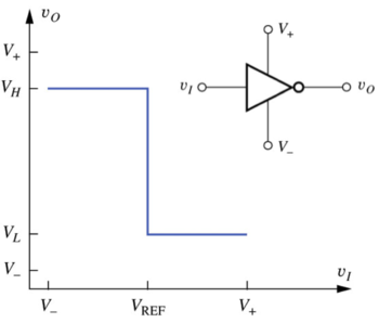 Figure 1: The ideal inverter voltage transfer characteristic (VTC)[1]. |
Static Design Metrics
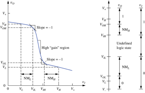 Figure : The non-ideal inverter voltage transfer characteristic (VTC)[1]. |
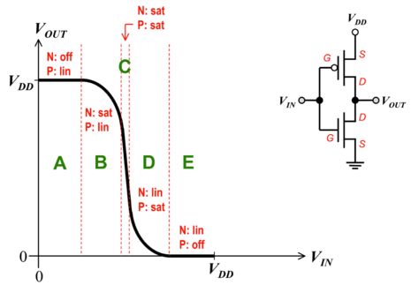 Figure : The CMOS inverter voltage transfer characteristic (VTC)[2]. |
Noise in Digital Circuits
Noise Rejection
Noise Margins
The Regenerative Property of Inverters
Inverter Delay
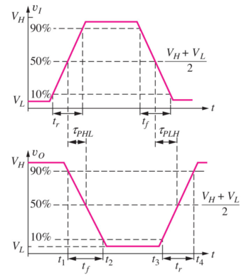 Figure: Logic delay definitions [1]. |
Power Dissipation
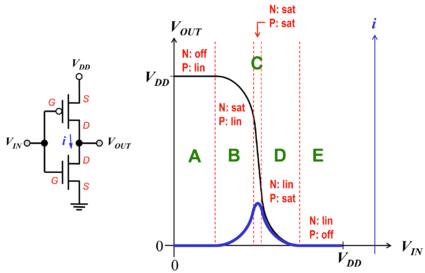 Figure : The CMOS switching current[3]. |
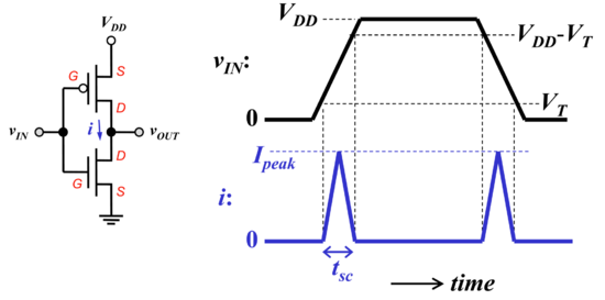 Figure : The CMOS transient power dissipation[3]. |


