Difference between revisions of "CoE 197U The CMOS Inverter"
Jump to navigation
Jump to search
| Line 27: | Line 27: | ||
{| | {| | ||
| − | |[[File:Timing definitions.png|thumb| | + | |[[File:Timing definitions.png|thumb|350px|Figure: Logic delay definitions <ref name="wu2014"/>.]] |
|- | |- | ||
|} | |} | ||
Revision as of 18:51, 5 March 2021
Contents
The Inverter Voltage Transfer Characteristics (VTC)
The Ideal Inverter VTC
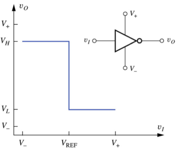 Figure : The ideal inverter voltage transfer characteristic (VTC)[1]. |
Static Design Metrics
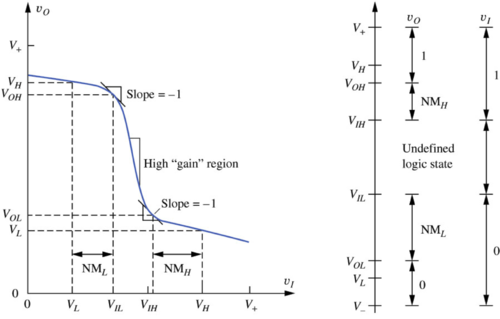 Figure : The non-ideal inverter voltage transfer characteristic (VTC)[1]. |
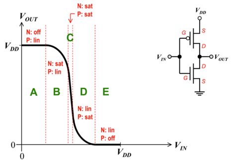 Figure : The CMOS inverter voltage transfer characteristic (VTC)[2]. |
Noise in Digital Circuits
Noise Rejection
Noise Margins
The Regenerative Property of Inverters
Inverter Delay
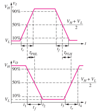 Figure: Logic delay definitions [1]. |
Power Dissipation
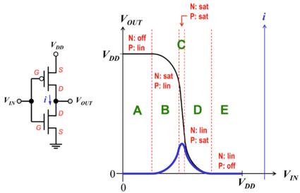 Figure : The CMOS switching current[3]. |
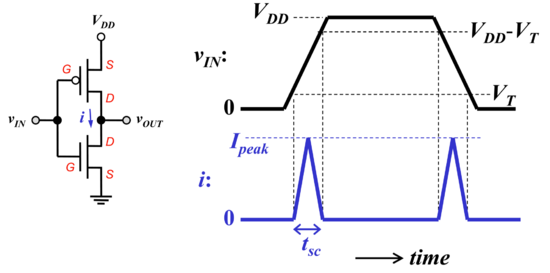 Figure : The CMOS transient power dissipation[3]. |