Difference between revisions of "220-A3.2"
| Line 21: | Line 21: | ||
The output resistance as a function of <math>V_{DS}</math> is shown in Figs. 3 and 4, for different values of <math>V_{GS}</math>. | The output resistance as a function of <math>V_{DS}</math> is shown in Figs. 3 and 4, for different values of <math>V_{GS}</math>. | ||
| + | |||
| + | {| | ||
| + | | [[File:NMOS gm corners.png|thumb|400px|Figure 2: NMOS transconductance.]] | ||
| + | | | ||
| + | | | ||
| + | |- | ||
| + | |} | ||
== Activity 1: Small Signal Models == | == Activity 1: Small Signal Models == | ||
Revision as of 09:34, 19 October 2020
Activity: MOS Small Signal Characteristics
- Instructions: This activity is structured as a tutorial with an activity at the end. Should you have any questions, clarifications, or issues, please contact your instructor as soon as possible.
- At the end of this activity, the student should be able to:
- Obtain the small signal parameters of NMOS and PMOS transistors.
Contents
Two-Port Small Signal Analysis
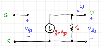
Most of the time, we are interested in the small signal behavior of our amplifiers, i.e. what happens to the amplifier voltages and currents as we introduce small disturbances (information carrying signals) at the input. To gain intuition and to facilitate circuit analysis using nonlinear devices, we linearize our circuits to obtain the two-port model shown in Fig. 1. For MOSFETs at low frequencies, the two-port model is composed of the transconductance, and the output resistance.
Transconductance
Transconductance is defined as:
-
(1)
-
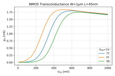
Graphically, this is the slope of the transfer characteristic curves. Thus, by numerically differentiating the vs. curve using this Python script, we can obtain the transconductance plot shown in Fig. 2.
Output Resistance
Similarly, we can take the derivative of the output characteristics to get the output resistance, which is defined as:
-
(2)
-
The output resistance as a function of is shown in Figs. 3 and 4, for different values of .
Activity 1: Small Signal Models
Answer the following questions:
- Given the transconductance plot in Fig. 2, why is there a peak in the transconductance curve? What is causing this?
- For the output resistance plot in Fig. 3, the effect of variations seem to be much larger for smaller values of . What do you think is causing this?
Activity 2: PMOS Small Signal Parameters
Numerically calculate and plot the transconductance and output resistance of a 45nm PMOS transistor with and . Compared to the NMOS plots, do you see any differences? Are the effects of process variations the same?
Report Guide
Write up a 2-3 page report with the annotated graphs showing the small signal parameters for both the NMOS and PMOS transistors, and submit the report via email.


