Difference between revisions of "Integrated Capacitors"
| Line 2: | Line 2: | ||
== Capacitance Geometries == | == Capacitance Geometries == | ||
| − | [[File:Parallel plate C.png|thumb| | + | [[File:Parallel plate C.png|thumb|400px|Figure 1: A parallel-plate capacitance.]] |
The parallel-plate capacitance of the structure shown in Fig. 1, is given by: | The parallel-plate capacitance of the structure shown in Fig. 1, is given by: | ||
| Line 11: | Line 11: | ||
=== Parasitic Capacitances === | === Parasitic Capacitances === | ||
In addition to the main parallel-plate capacitance, <math>C</math>, we would get the following parasitic capacitances: | In addition to the main parallel-plate capacitance, <math>C</math>, we would get the following parasitic capacitances: | ||
| − | * A '''bottom plate parasitic capacitance''' between the bottom plate and the substrate. | + | * A '''bottom plate parasitic capacitance''', <math>C_\mathrm{bottom}</math>, between the bottom plate and the substrate. |
| − | * '''fringing capacitances''', due to the fringing electric fields between the: | + | * Perimeter-dependent '''fringing capacitances''', due to the fringing electric fields between the: |
| − | *# top plate and bottom plate, resulting in an increase in the main capacitance predicted by the parallel-plate expression in Eq. 1, | + | *# top plate and bottom plate, <math>C_1</math>, resulting in an increase in the main capacitance predicted by the parallel-plate expression in Eq. 1, |
| − | *# top plate and substrate, adding a ''top plate parasitic capacitance'', and | + | *# top plate and substrate, <math>C_2</math>, adding a ''top plate parasitic capacitance'', and |
| − | *# bottom plate and substrate, again adding to the capacitance predicted by our parallel-plate formula. | + | *# bottom plate and substrate, <math>C_3</math>, again adding to the capacitance predicted by our parallel-plate formula. |
| − | Note that it is much harder to model and predict the capacitance due to the non-uniform fringing electric fields. We can reduce the effects of the fringing fields by making the main capacitance much larger than the parasitic fringing capacitances. | + | Note that it is much harder to model and predict the capacitance due to the non-uniform fringing electric fields. We can reduce the effects of the fringing fields by making the main capacitance much larger than the parasitic fringing capacitances by minimizing the perimeter of the parallel-plate structure. |
== Layout and Matching == | == Layout and Matching == | ||
Revision as of 05:47, 22 September 2020
Similar to resistors, in a CMOS process optimized for digital circuits, capacitances are treated as parasitic devices that degrade the performance of digital circuits, except in specialized cases such as memory circuits. However, in analog design, we often need capacitors with very well-controlled capacitance values.
Capacitance Geometries
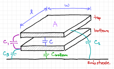
The parallel-plate capacitance of the structure shown in Fig. 1, is given by:
-
(1)
-
Where is the capacitance density of a particular layer, is the permittivity of the dielectric or insulating material, is the thickness of the dielectric, and is the overlap area of the parallel-plate.
Parasitic Capacitances
In addition to the main parallel-plate capacitance, , we would get the following parasitic capacitances:
- A bottom plate parasitic capacitance, , between the bottom plate and the substrate.
- Perimeter-dependent fringing capacitances, due to the fringing electric fields between the:
- top plate and bottom plate, , resulting in an increase in the main capacitance predicted by the parallel-plate expression in Eq. 1,
- top plate and substrate, , adding a top plate parasitic capacitance, and
- bottom plate and substrate, , again adding to the capacitance predicted by our parallel-plate formula.
Note that it is much harder to model and predict the capacitance due to the non-uniform fringing electric fields. We can reduce the effects of the fringing fields by making the main capacitance much larger than the parasitic fringing capacitances by minimizing the perimeter of the parallel-plate structure.


