Difference between revisions of "Introduction to EE 229"
Jump to navigation
Jump to search

| Line 10: | Line 10: | ||
Let's get started! | Let's get started! | ||
| − | == | + | == The Design of RF Transceivers == |
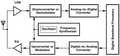
[[File:RF Transceiver.png|thumb|400px|Figure 1: A generic RF transceiver<ref name="Razavi2012">Behzad Razavi, ''RF Microelectronics (2nd Edition)'', Prentice Hall Press, 2011, USA.</ref>.]] | [[File:RF Transceiver.png|thumb|400px|Figure 1: A generic RF transceiver<ref name="Razavi2012">Behzad Razavi, ''RF Microelectronics (2nd Edition)'', Prentice Hall Press, 2011, USA.</ref>.]] | ||
| − | The objective of an RF transceiver is to transmit and receive information. To perform this task, however, requires concepts, technologies, and interactions from and among many fields, and some of these fields | + | The objective of an RF transceiver is to transmit and receive information. To perform this task, however, requires concepts, technologies, and interactions from and among many fields, and some of these fields might not directly related to IC design. The task itself is relatively complex, with trade-offs and optimizations spanning various domains and levels of abstractions. |
| + | |||
| + | Fig. 1 shows a generic RF transceiver block diagram, showing: | ||
| + | * The transmit path, showing of basic system components needed to convert digital data into its analog form, modulate the signal, up-convert it from baseband to some center frequency, and finally send it to the antenna using a power amplifier. | ||
| + | * The receive path, where the signal is detected the low-noise amplifier, then down-converted back to baseband from a certain center frequency, then converted into the appropriate digital representation in preparation for further processing. | ||
== A Short Review == | == A Short Review == | ||
Revision as of 02:01, 10 September 2020
Welcome to EE 229!
Since we are offering this class remotely, there will be many changes to our normal course delivery:
- There will be no face-to-face lecture classes. All the material will be made available via this site.
- There will be more emphasis on student-centric activities, e.g. analysis, design, and simulations. Thus, you will be mostly "learning by doing". In this context, we will set aside an hour every week for consultations and questions via video-conferencing.
- Grades will be based on the submitted deliverables from the activities. Though we will not be very strict regarding the deadlines, it is a good idea to keep up with the class schedule and avoid cramming later in the semester.
Please remember that this semester is very different from those before, and please make sure you inform me if you have any issues or difficulties regarding the class. Also, keep in mind that you will need to pay a bit more attention to your time management as it will play a critical role during the course of the semester.
Let's get started!
Contents
The Design of RF Transceivers

Figure 1: A generic RF transceiver[1].
The objective of an RF transceiver is to transmit and receive information. To perform this task, however, requires concepts, technologies, and interactions from and among many fields, and some of these fields might not directly related to IC design. The task itself is relatively complex, with trade-offs and optimizations spanning various domains and levels of abstractions.
Fig. 1 shows a generic RF transceiver block diagram, showing:
- The transmit path, showing of basic system components needed to convert digital data into its analog form, modulate the signal, up-convert it from baseband to some center frequency, and finally send it to the antenna using a power amplifier.
- The receive path, where the signal is detected the low-noise amplifier, then down-converted back to baseband from a certain center frequency, then converted into the appropriate digital representation in preparation for further processing.
A Short Review
Power and Gain
Time Variance
References
- ↑ Behzad Razavi, RF Microelectronics (2nd Edition), Prentice Hall Press, 2011, USA.