|
|
| (One intermediate revision by the same user not shown) |
| Line 42: |
Line 42: |
| | Again note that we are referring to random noise and not interference or distortion. | | Again note that we are referring to random noise and not interference or distortion. |
| | | | |
| − | == Resistor Noise == | + | == Noise Figure == |
| − | Due to the random thermal motion of charge carriers, we get '''thermal noise''', and we observe it as voltage and current noise in resistive circuit elements that is proportional to absolute temperature. We expect this to be the case since at higher temperatures, electrons and holes have higher energy, leading to larger instantaneous velocities, and thus larger excursions from the mean velocity, e.g. from an electric field-induced drift velocity.
| + | [[File:RF source with noise.png|thumb|350px|Figure 4: A "noisy" RF source.]] |
| | + | The noise figure (NF) measures the degradation of SNR in a circuit or block. The noise figure is defined as: |
| | | | |
| − | === Modeling Thermal Noise in Resistors ===
| + | {{NumBlk|::|<math>F=\frac{\mathrm{SNR_{in}}}{\mathrm{SNR_{out}}}</math>|{{EquationRef|7}}}} |
| − | [[File:R noise model.png|thumb|350px|Figure 4: Resistor noise generators.]]
| |
| − | Consider the noisy resistor in Fig. 4. We can model this as a noiseless resistor in series with a voltage noise generator, or a noiseless resistor in parallel with a current noise generator. Since we cannot predict the voltage or current noise at any point in time, we can instead specify the noise mean square voltage spectral density over a unit bandwidth, <math>\Delta f</math>:
| |
| | | | |
| − | {{NumBlk|::|<math>\overline{v^2_n} = 4kTR \Delta f</math>|{{EquationRef|7}}}}
| + | Expressed in dB, we get: |
| | | | |
| − | Where <math>k</math> is Boltzmann's constant, equal to <math>1.38064852 \times 10^{-23}\mathrm{\tfrac{J}{K}}</math> and <math>T</math> is the temperature in Kelvin. The total integrated noise power is then:
| + | {{NumBlk|::|<math>\mathrm{NF}=10\log\frac{\mathrm{SNR_{in}}}{\mathrm{SNR_{out}}}</math>|{{EquationRef|8}}}} |
| | | | |
| − | {{NumBlk|::|<math>\overline{v^2_{n,T}} = \int_B \left(\frac{\overline{v^2_n}}{\Delta f}\right) df = \int_B 4kTR\, df= 4kTRB</math>|{{EquationRef|8}}}}
| + | We use <math>F</math> and <math>\mathrm{NF}</math> to distinguish between the dB and non-dB values of noise figure. Note that some texts call <math>F</math> the ''noise factor''. In measuring or calculating the noise figure, we specify a standard input noise level, generated by a source resistance, <math>R_S</math>, at a set temperature. For example, in RF systems, we typically set <math>R_S=50\mathrm{\Omega}</math> and <math>T=293\mathrm{K}</math>, as seen in Fig. 4. More on this when we cover the origins of electronic noise. |
| | | | |
| − | Where <math>B</math> is the observation bandwidth. Alternatively, we can specify the total integrated noise power from the noise current generator:
| + | === Amplifier Noise Figure === |
| | + | [[File:Noise amp model.png|thumb|350px|Figure 5: A "noisy" amplifier.]] |
| | + | Consider the amplifier model in Fig. 5, with input signal <math>S_i</math>, power gain <math>G</math>, and output signal <math>S_o</math>. If the power of the input signal is <math>P_\mathrm{signal}</math>, and <math>N_S</math> is the noise power at the input, we can write the input SNR as: |
| | | | |
| − | {{NumBlk|::|<math>\overline{i^2_{n,T}} = 4kTGB = \frac{4kTB}{R}</math>|{{EquationRef|9}}}} | + | {{NumBlk|::|<math>\mathrm{SNR_{in}}=\frac{P_\mathrm{signal}}{N_S}</math>|{{EquationRef|9}}}} |
| | | | |
| − | [[File:R spectral density.png|thumb|350px|Figure 5: The resistor noise power spectral density.]]
| + | Since amplifier will amplify both the signal and the noise, the output SNR is then: |
| − | Thermal noise is ''white'' noise, since <math>\tfrac{\overline{v^2_n}}{\Delta f}=4kTR</math> is constant over frequency, and hence the noise generators have ''white'' power spectral densities, as shown in Fig. 5. Just like any small signal, the shape of the power spectral density can be shaped by the frequency response of the rest of the circuit.
| |
| | | | |
| − | Also note that the polarity of the noise generators are intentionally not specified in the symbols shown in Fig. 4, since the noise voltage or current can take on positive or negative values at any given time.
| + | {{NumBlk|::|<math>\mathrm{SNR_{out}}=\frac{G\cdot P_\mathrm{signal}}{G\cdot N_S + N_\mathrm{amp,o}} = \frac{P_\mathrm{signal}}{N_S + \frac{N_\mathrm{amp,o}}{G}} = \frac{P_\mathrm{signal}}{N_S + N_\mathrm{amp,i}}</math>|{{EquationRef|10}}}} |
| | | | |
| − | For example, a resistor with <math>R=10\mathrm{k\Omega}</math> at <math>T=20^\circ C=293K</math>, the voltage noise power is:
| + | Where <math>N_\mathrm{amp,o}</math> is the noise power at the output of the amplifier when there is no input, and <math>N_\mathrm{amp,i}=\tfrac{N_\mathrm{amp,o}}{G}</math> is the ''input referred'' noise of the amplifier. The noise figure is then: |
| | | | |
| − | {{NumBlk|::|<math>\overline{v^2_{n,T}}=4kTRB=1.62\times 10^{-16}\cdot B</math>|{{EquationRef|10}}}} | + | {{NumBlk|::|<math>F=\frac{\mathrm{SNR_{in}}}{\mathrm{SNR_{out}}}=\frac{P_\mathrm{signal}}{N_S}\cdot\frac{N_S + N_\mathrm{amp,i}}{P_\mathrm{signal}}=1+\frac{N_\mathrm{amp,i}}{N_S} \geq 1</math>|{{EquationRef|11}}}} |
| | | | |
| − | Which gives us:
| + | Thus, any real system adds noise and degrades the SNR, resulting in a noise figure greater than one. We only get <math>F=1</math> if we have a noiseless amplifier. |
| | | | |
| − | {{NumBlk|::|<math>v_\mathrm{n,rms}=\sqrt{\overline{v^2_{n,T}}}=\sqrt{4kTRB}=1.27\times 10^{-8}\cdot \sqrt{B}</math>|{{EquationRef|11}}}}
| + | === Noise Figure of Cascaded Blocks === |
| | + | [[File:Cascaded amp noise.png|thumb|400px|Figure 6: Noise in cascaded amplifiers.]] |
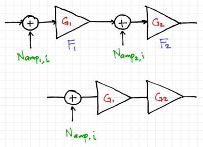
| | + | Two amplifiers are cascaded as shown in Fig. 6. Assume that the amplifiers are properly matched such that the overall power gain is <math>G=G_1\cdot G_2</math>, with noise figures <math>F_1=1+\tfrac{N_{\mathrm{amp_1,i}}}{N_S}</math> and <math>F_2=1+\tfrac{N_{\mathrm{amp_2,i}}}{N_S}</math>. Thus, the input referred noise of amplifier 2 is: |
| | | | |
| − | For a measurement bandwidth of <math>B=1\mathrm{MHz}</math>, we get <math>v_\mathrm{n,rms}=13\,\mathrm{\mu V}</math>. This is the smallest voltage, or the ''minimum detectable signal'' we can resolve across this resistor with this bandwidth, i.e. the smallest voltage we can distinguish from the thermal noise of the resistor.
| + | {{NumBlk|::|<math>N_\mathrm{amp_2,i} = N_S \left(F_2 - 1\right)</math>|{{EquationRef|12}}}} |
| | | | |
| − | === Noise in Resistor Circuits ===
| + | And the total input referred noise is composed of the input referred noise of amplifier 1 plus the noise of amplifier 2 divided by the power gain of amplifier 1: |
| − | Consider two noisy resistors in series, as shown in Fig. 6. The equivalent resistance of the series circuit is <math>R=R_1 + R_2</math>, and since we can sum the voltage noise powers, we get:
| |
| | | | |
| − | {{NumBlk|::|<math>\overline{v^2_R} = \overline{v^2_{R_1}} + \overline{v^2_{R_2}} = 4kTR_1 \Delta f + 4kTR_1 \Delta f = 4kT\left(R_1 + R_2\right)\Delta f = 4kTR\Delta f</math>|{{EquationRef|12}}}} | + | {{NumBlk|::|<math>N_\mathrm{amp,i} = N_\mathrm{amp_1,i} + \frac{N_\mathrm{amp_2,i}}{G_1} = N_S \left(F_1 - 1\right) + \frac{N_S \left(F_2 - 1\right)}{G_1}</math>|{{EquationRef|13}}}} |
| | | | |
| − | It is important to remember that the noise power is additive, but the noise voltages and currents are not, since we do not know the phase of these signals at a given point in time. Similarly, for the parallel resistor circuit in Fig. 7, the equivalent conductance is <math>G=G_1 + G_2</math>, and the resulting equivalent current noise generator is:
| + | Thus, the overall noise figure is: |
| | | | |
| − | {{NumBlk|::|<math>\overline{i^2_G} = \overline{i^2_{G_1}} + \overline{i^2_{G_2}}= 4kTG_1 \Delta f + 4kTG_1 \Delta f = 4kT\left(G_1 + G_2\right) \Delta f = 4kTG\Delta f</math>|{{EquationRef|13}}}} | + | {{NumBlk|::|<math>F = 1 + \frac{N_\mathrm{amp,i}}{N_S} = 1+ \left(F_1 - 1\right) + \frac{\left(F_2 - 1\right)}{G_1} = F_1 + \frac{F_2 -1}{G_1}</math>|{{EquationRef|14}}}} |
| | | | |
| − | {|
| + | In general, for <math>m</math> cascaded amplifiers, the overall noise figure is: |
| − | | [[File:Series R noise.png|thumb|300px|Figure 6: Equivalent noise generators for resistors in series.]]
| |
| − | | [[File:Parallel R noise.png|thumb|500px|Figure 7: Equivalent noise generators for resistors in parallel.]]
| |
| − | |-
| |
| − | |}
| |
| | | | |
| − | In adding the noise powers, we assumed that the noise generators are independent of each other, i.e. the noise sources are uncorrelated. We will look at the case of correlated noise sources later.
| + | {{NumBlk|::|<math>F = F_1 + \frac{F_2 -1}{G_1} + \frac{F_3 -1}{G_1 G_2} + \frac{F_4 -1}{G_1 G_2 G_3} + \ldots + \frac{F_m -1}{G_1 G_2 \cdots G_{m-1}}</math>|{{EquationRef|15}}}} |
| | | | |
| − | [[File:Noise Thevenin.png|thumb|500px|Figure 8: The equivalent noise of an arbitrary circuit with resistors and independent sources.]]
| + | This is known as ''Friis' Equation''. Thus, the noise contribution of each successive stage is progressively smaller. This makes the noise of the first stage the dominant noise source, and hence, the most important. |
| − | Extending these definitions to any arbitrary resistive circuit, we can determine the equivalent Thevenin or Norton equivalent circuit, as illustrated in Fig. 8, as well as the noise associated with the Thevenin resistance, <math>R_T</math>, as:
| |
| − | | |
| − | {{NumBlk|::|<math>\overline{v^2_{R_T}}= 4kTR_T \Delta f</math>|{{EquationRef|14}}}}
| |
| − | | |
| − | == Diode Noise ==
| |
| − | [[File:Diode noise.png|thumb|300px|Figure 9: Diode noise.]]
| |
| − | Shot noise is the random movement of quantized charges flowing through a forward-biased PN junction. The shot noise power in a diode, over a unit bandwidth <math>\Delta f</math>, shown in Fig. 9, is given by:
| |
| − | | |
| − | {{NumBlk|::|<math>\overline{i^2_n} = 2qI_D \Delta f</math>|{{EquationRef|15}}}}
| |
| − | | |
| − | Where <math>q = 1.602\times 10^{-19}\,\mathrm{C}</math>, <math>I_D</math> is the DC current flowing through the diode. Shot noise has a white power spectral density similar to thermal noise, however, it is independent of temperature and instead, is proportional to the DC diode current. Since noise, in general, can be considered a "small signal", we normally include the noise generators in the diode small signal model, where <math>r_d = \left(\tfrac{\partial I_D}{\partial V_D}\right)^{-1}</math> is the diode small signal equivalent resistance.
| |
| − | | |
| − | == BJT Noise ==
| |
| − | [[File:BJT noise model.png|thumb|500px|Figure 10: The BJT small signal model with noise generators.]]
| |
| − | In a bipolar junction transistor (BJT), both PN junctions produce shot noise. The noise at the base-emitter junction is:
| |
| − | | |
| − | {{NumBlk|::|<math>\overline{i^2_b} = 2qI_B \Delta f</math>|{{EquationRef|16}}}}
| |
| − | | |
| − | And similarly, for the collector-base junction, we get:
| |
| − | | |
| − | {{NumBlk|::|<math>\overline{i^2_c} = 2qI_C \Delta f</math>|{{EquationRef|17}}}}
| |
| − | | |
| − | Fig. 10 shows the small signal model of the BJT, showing the shot noise generators, <math>\overline{i^2_b}</math> and <math>\overline{i^2_c}</math>, and the thermal noise generators for the ''physical'' terminal resistances, <math>r_b</math>, <math>r_e</math>, and <math>r_c</math>.
| |
| − | | |
| − | Note that the small signal resistances <math>r_\pi</math> and <math>r_o</math> are not physical resistors. These small signal resistors are used to model mechanisms such as recombination and base-width modulation, and thus, do not generate noise.
| |
| − | | |
| − | == MOSFET Noise ==
| |
| − | [[File:MOSFET id spectral density.png|thumb|400px|Figure 11: The power spectral density of <math>\overline{i^2_d}</math>.]]
| |
| − | [[File:MOSFET noise model.png|thumb|500px|Figure 12: The MOSFET small signal model with noise generators.]]
| |
| − | The MOSFET has two noise mechanisms present: (1) thermal noise due to the channel and terminal resistances, and (2) '''flicker noise''' due to vacant energy levels or ''surface states'' or ''traps'' in the interface between the channel and the gate oxide layer. These surface states trap charges for a short period of time, and is then released, producing random changes in the current. Since the probability of charges getting trapped in these surface states is (approximately) inversely proportional to frequency, flicker noise is also known as ''<math>\tfrac{1}{f}</math> noise''.
| |
| − | | |
| − | We can then express the drain current noise of a MOSFET as the sum of the thermal noise and flicker noise components, over a bandwidth of <math>\Delta f</math>, respectively:
| |
| − | | |
| − | {{NumBlk|::|<math>\overline{i^2_d} = 4kT\gamma g_{ds0} \Delta f + K_f \frac{I_D^a}{C_{\mathrm{ox}} L_{\mathrm{eff}}^2 f^e} \Delta f</math>|{{EquationRef|18}}}}
| |
| − | | |
| − | Note that <math>\gamma</math> is known as the ''excess noise coefficient'', and is equal to <math>\tfrac{2}{3}</math> for long channel devices, <math>g_{ds0}</math> is the drain-source conductance in the triode region, <math>C_\mathrm{ox}</math> is the oxide capacitance, and <math>L_\mathrm{eff}</math> is the effective length of the MOSFET. The constants <math>K_f</math>, <math>a</math>, and <math>e</math> are process dependent, and are usually determined empirically. In most cases, using <math>g_{ds0}</math> is not very convenient. For long channel devices with <math>V_{DS}=0</math>:
| |
| − | | |
| − | {{NumBlk|::|<math>g_{ds0} = \frac{\partial I_D}{\partial V_{DS}}=\mu C_\mathrm{ox}\frac{W}{L}\left(V_{GS}-V_{TH}\right) = g_m</math>|{{EquationRef|19}}}}
| |
| − | | |
| − | This allows us to use the transconductance instead. However, for short-channel devices, <math>g_m\ne g_{ds0}</math>. To correct for this, we can introduce a new parameter <math>\alpha=\tfrac{g_m}{g_{ds0}}</math>, leading to an alternative expression for the drain current noise: | |
| − | | |
| − | {{NumBlk|::|<math>\overline{i^2_d} = 4kT\frac{\gamma}{\alpha} g_m \Delta f + K_f \frac{I_D^a}{C_{\mathrm{ox}} L_{\mathrm{eff}}^2 f^e} \Delta f</math>|{{EquationRef|20}}}}
| |
| − | | |
| − | Fig. 11 shows the power spectral density of the MOSFET drain current noise. Note that the spectral density of flicker noise is not white since there is more power in the lower frequencies, thus the term ''pink noise'' in reference to the low frequency colors of the visible electromagnetic spectrum. Since the spectral density is not white, we cannot just multiply the spectral density with the bandwidth <math>B</math>, but instead, we need to integrate over <math>\Delta f</math> to get the total area under the spectral density curve. The noise spectral density in a narrow frequency band <math>\Delta f</math> is also called ''spot noise''. Another useful metric is the ''flicker noise corner'', <math>f_c</math> in Fig. 3, and it is defined as the frequency when the thermal noise component is equal to the flicker noise component. Below the flicker noise corner frequency, flicker noise dominates, while above <math>f_c</math>, thermal noise dominates.
| |
| − | | |
| − | The small signal model of the MOSFET, including the noise generators, is shown in Fig. 12. Once again, physical resistors like the terminal resistances <math>r_g</math>, <math>r_s</math>, and <math>r_d</math> generate noise, while the output impedance, <math>r_o</math>, does not. In RF applications, we are mostly interested in <math>\overline{i^2_d}</math> and <math>\overline{v^2_{r_g}}</math>.
| |
In this module, we consider the noise generated by the electronic devices themselves due to the (1) random motion of electrons due to thermal energy and (2) the discreteness of electric charge. We see this as thermal noise in resistances, and shot noise in PN junctions. In MOS transistors, we also see flicker noise. This noise is not fundamental, but is due to the way MOS transistors are manufactured, This added uncertainty in the voltages and currents limit the smallest signal amplitude or power that our circuits can detect and/or process, limiting the transmission range and power requirements for reliable communications. Note that purely reactive elements, i.e. ideal inductors and capacitors, do not generate noise, but they can shape the frequency spectrum of the noise.
Modeling Noise

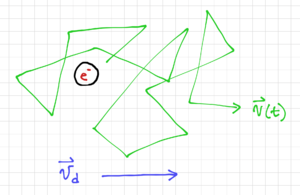
Figure 1: Random movement of an electron in an electric field.
Since electronic noise is random, we cannot predict its value at any given time. However, we can describe noise in terms of its aggregate characteristics or statistics, such as its probability distribution function (pdf). As expected from the Central Limit Theorem, the pdf of the random movement of many electrons would approach a Gaussian distribution with zero mean since the electrons will move around instantaneously, but without any excitation, it will, on the average, stay in the same point in space. If we add an electric field, then the electron will move with an average drift velocity,  , but at any point in time, it would be moving with an instantaneous velocity
  , as shown in Fig. 1. Note that
  is the electron mobility.
Noise Power
Aside from the mean, to describe a zero-mean Gaussian random variable,  , we need the variance,
  , or the mean of
  . For random voltages or currents,
  , this is equal to the average power over time, normalized to
  :
:
-
 |
|
(1)
|

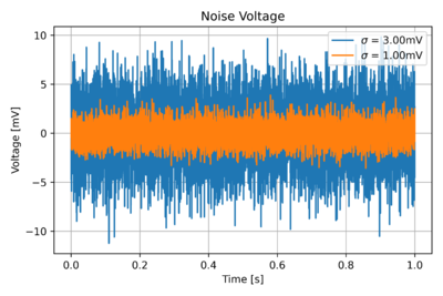
Figure 2: Zero-mean noise signals in time with different variances.
Thus, to describe noise, we can use its variance, or equivalently its average power. Fig. 2 illustrates the difference between two noise signals with different variances. Recall that  , the square root of the variance, is the standard deviation.
Consider a noise voltage in time,  , similar to the ones depicted in Fig. 2. The mean is then:
-
 |
|
(2)
|
The variance, however, is non-zero:
-
 |
|
(3)
|
We can also calculate the root-mean-square or RMS as:
-
 |
|
(4)
|
Noise Power Spectrum

Figure 3: The power spectral density of white noise.
We can also examine the noise in the frequency domain, specifically, how noise power is distributed over frequency. Many noise sources are white, i.e. the noise power is distributed evenly across all frequencies, as seen in Fig. 3. Thus, white noise is totally unpredictable in time since there is no correlation between the noise at time  and the noise at time
  , no matter how small
  is, since the likelihood of a high frequency change (small
  ) and a low frequency change (large
  ) are the same.
The noise power should be the same, whether we obtain it from the time or frequency domain. Thus, calculating the noise power in time and in frequency, and equating the two, we get:
-
 |
|
(5)
|
Where  is the noise power spectral density in
  . An alternate representation of the noise spectrum is the root spectral density,
  , with units of
  .
.
Signal-to-Noise Ratio
In general, we try to maximize the signal-to-noise ratio (SNR) in a communication system. For an average signal power  , and an average noise power
  , the SNR in dB is defined as:
-
 |
|
(6)
|
Again note that we are referring to random noise and not interference or distortion.
Noise Figure

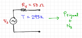
Figure 4: A "noisy" RF source.
The noise figure (NF) measures the degradation of SNR in a circuit or block. The noise figure is defined as:
-
 |
|
(7)
|
Expressed in dB, we get:
-
 |
|
(8)
|
We use  and
and  to distinguish between the dB and non-dB values of noise figure. Note that some texts call
  the noise factor. In measuring or calculating the noise figure, we specify a standard input noise level, generated by a source resistance,
  , at a set temperature. For example, in RF systems, we typically set
  and
and  , as seen in Fig. 4. More on this when we cover the origins of electronic noise.
Amplifier Noise Figure

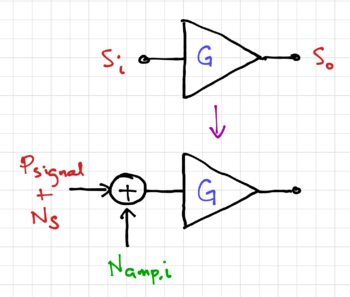
Figure 5: A "noisy" amplifier.
Consider the amplifier model in Fig. 5, with input signal  , power gain
  , and output signal
  . If the power of the input signal is
  , and
, and  is the noise power at the input, we can write the input SNR as:
-
 |
|
(9)
|
Since amplifier will amplify both the signal and the noise, the output SNR is then:
-
 |
|
(10)
|
Where  is the noise power at the output of the amplifier when there is no input, and
  is the input referred noise of the amplifier. The noise figure is then:
-
 |
|
(11)
|
Thus, any real system adds noise and degrades the SNR, resulting in a noise figure greater than one. We only get  if we have a noiseless amplifier.
Noise Figure of Cascaded Blocks

Figure 6: Noise in cascaded amplifiers.
Two amplifiers are cascaded as shown in Fig. 6. Assume that the amplifiers are properly matched such that the overall power gain is  , with noise figures
  and
and  . Thus, the input referred noise of amplifier 2 is:
-
 |
|
(12)
|
And the total input referred noise is composed of the input referred noise of amplifier 1 plus the noise of amplifier 2 divided by the power gain of amplifier 1:
-
 |
|
(13)
|
Thus, the overall noise figure is:
-
 |
|
(14)
|
In general, for  cascaded amplifiers, the overall noise figure is:
-
 |
|
(15)
|
This is known as Friis' Equation. Thus, the noise contribution of each successive stage is progressively smaller. This makes the noise of the first stage the dominant noise source, and hence, the most important.
