Difference between revisions of "229-A2.2"
| (13 intermediate revisions by the same user not shown) | |||
| Line 1: | Line 1: | ||
Activity: '''Noise Analysis''' | Activity: '''Noise Analysis''' | ||
| − | * '''Instructions''': This activity is structured as a tutorial with | + | * '''Instructions''': This activity is structured as a tutorial with an activity at the end. Should you have any questions, clarifications, or issues, please contact your instructor as soon as possible. |
* At the end of this activity, the student should be able to: | * At the end of this activity, the student should be able to: | ||
# Understand and observe the effects of noise in electronic circuits. | # Understand and observe the effects of noise in electronic circuits. | ||
| Line 68: | Line 68: | ||
== Activity: Noise in MOSFETs == | == Activity: Noise in MOSFETs == | ||
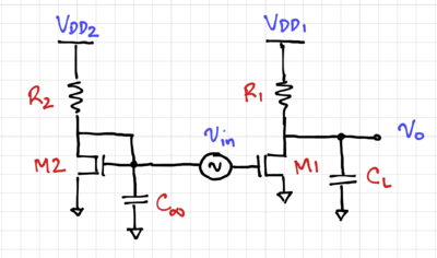
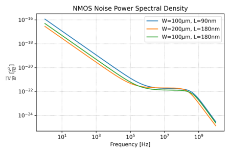
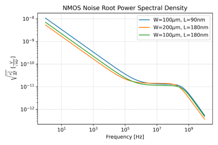
| − | Let us use the NMOS current mirror in Fig. 4 to simulate the drain current noise in of the 45nm NMOS transistor '''M1'''. Using this SPICE netlist and Python script, we can plot the power spectral density and root spectral density of the drain current, as shown in Figs. 5 and 6, for three different sizes. Note that we did not include the resistor noise in the simulation using the '''noisy=0''' directive. | + | [[File:NMOS noise.png|thumb|400px|Figure 4: A noisy NMOS current mirror.]] |
| + | Let us use the NMOS current mirror in Fig. 4 to simulate the drain current noise in of the [https://github.com/louisalarcon/ee229/blob/master/src/45nm_NMOS_bulk69327.pm 45nm NMOS transistor] '''M1'''. Using this SPICE [https://github.com/louisalarcon/ee229/blob/master/src/MOS_noise.sp netlist] and Python [https://github.com/louisalarcon/ee229/blob/master/src/a2.2-2.py script], we can plot the power spectral density and root spectral density of the drain current, as shown in Figs. 5 and 6, for three different sizes. Note that we did not include the resistor noise in the simulation using the '''noisy=0''' directive. | ||
| − | # Are the plots in Figs. 5 and 6 what you expect given the three different transistor sizes? | + | # Are the plots in Figs. 5 and 6 what you expect given the three different transistor sizes? Specifically, the frequency breakpoints and the relative values of the flicker noise and thermal noise levels as a function of transistor size. |
| − | # Show that the capacitor <math>C_\infty</math> prevents the noise | + | # Show that the capacitor <math>C_\infty</math> prevents the noise of '''M2''' from reaching '''M1'''. Verify this by removing <math>C_\infty</math> and observing the output noise spectrum. |
| − | # Using the the simulation data, estimate the values of <math>\tfrac{\gamma}{\alpha}</math> and <math>K_f</math>. | + | # Using the the simulation data, estimate the values of <math>\tfrac{\gamma}{\alpha}</math> and <math>\tfrac{K_f}{C_\mathrm{ox}}</math>, assuming <math>\alpha=1</math> and <math>e=1</math>. A convenient way to do this is to use SciPy's [https://scipy-lectures.org/intro/scipy/auto_examples/plot_curve_fit.html curve_fit] function. |
# Calculate the value of the noise corner frequency, <math>f_c</math>, and compare this with the simulation data. | # Calculate the value of the noise corner frequency, <math>f_c</math>, and compare this with the simulation data. | ||
| − | # Derive an expression for the total output integrated ''voltage'' noise, <math>\overline{v_{o,T}^2}</math>. Is this consistent with the simulation results? Ignore the terminal resistances for now. | + | # Derive an expression for the total output integrated ''voltage'' noise, <math>\overline{v_{o,T}^2}</math>. Is this consistent with the simulation results? What are the possible sources of error? Ignore the terminal resistances for now. |
| − | # Repeat the activity for a 45nm PMOS transistor. Note that you need to create a PMOS current mirror, and set the drain currents to approximately the same values as their NMOS counterparts. | + | # Repeat the activity for a [https://github.com/louisalarcon/ee229/blob/master/src/45nm_PMOS_bulk47755.pm 45nm PMOS transistor]. Note that you need to create a PMOS current mirror, and set the drain currents to approximately the same values as their NMOS counterparts. |
| + | |||
| + | {| | ||
| + | | [[File:MOS noise spectrum.png|thumb|450px|Figure 5: The NMOS output voltage noise spectral density.]] | ||
| + | | [[File:MOS noise root spectrum.png|thumb|450px|Figure 6: The NMOS output voltage noise root spectral density.]] | ||
| + | |- | ||
| + | |} | ||
=== Report Guide === | === Report Guide === | ||
Write a short report explaining your answers to the questions above, and submit it via email. | Write a short report explaining your answers to the questions above, and submit it via email. | ||
Latest revision as of 11:18, 11 October 2020
Activity: Noise Analysis
- Instructions: This activity is structured as a tutorial with an activity at the end. Should you have any questions, clarifications, or issues, please contact your instructor as soon as possible.
- At the end of this activity, the student should be able to:
- Understand and observe the effects of noise in electronic circuits.
Example: Simulating the Noise of a Resistor
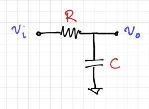
Consider a simple RC circuit shown in Fig. 1. The noise generated by the resistor is:
-
(1)
-
Thus, for a resistor and a temperature , and with , the spot noise is equal to:
-
(2)
-
Thus, for a capacitor , the total output integrated noise, shaped by the transfer function of the RC circuit is:
-
(3)
-
Or equivalently,
-
(4)
-
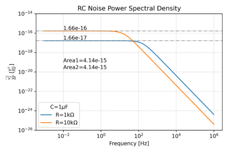
If we change the value of the resistor to , the resistor spot noise changes to:
-
(5)
-
But the total integrated noise should remain the same since the bandwidth of the RC circuit is reduced by the same amount. To verify our calculations, we can use SPICE to simulate the noise of the RC circuit. Using this netlist and this Python script, we get the following ngspice results:
******
** ngspice-31 : Circuit level simulation program
** The U. C. Berkeley CAD Group
** Copyright 1985-1994, Regents of the University of California.
** Please get your ngspice manual from http://ngspice.sourceforge.net/docs.html
** Please file your bug-reports at http://ngspice.sourceforge.net/bugrep.html
******
ngspice 1 -> source RC_noise.sp

Circuit: * noise simulations

Doing analysis at TEMP = 27.000000 and TNOM = 27.000000


No. of Data Rows : 9001

No. of Data Rows : 1
onoise_total = 4.143579e-15
Doing analysis at TEMP = 27.000000 and TNOM = 27.000000


No. of Data Rows : 9001

No. of Data Rows : 1
onoise_total = 4.143808e-15
ngspice 2 ->
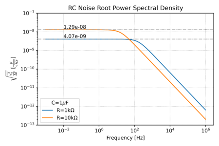
Note that since the noise voltages and currents are relatively small, we need to adjust the SPICE calculation tolerances, as was done in our netlist. We can use our Python script to plot the output noise spectral density, as shown in Fig. 2, and the root spectral density, seen in Fig. 3.
As expected, the total integrated output noise is independent of the value of the resistor, and only depends on the value of the capacitor.
Activity: Noise in MOSFETs
Let us use the NMOS current mirror in Fig. 4 to simulate the drain current noise in of the 45nm NMOS transistor M1. Using this SPICE netlist and Python script, we can plot the power spectral density and root spectral density of the drain current, as shown in Figs. 5 and 6, for three different sizes. Note that we did not include the resistor noise in the simulation using the noisy=0 directive.
- Are the plots in Figs. 5 and 6 what you expect given the three different transistor sizes? Specifically, the frequency breakpoints and the relative values of the flicker noise and thermal noise levels as a function of transistor size.
- Show that the capacitor prevents the noise of M2 from reaching M1. Verify this by removing and observing the output noise spectrum.
- Using the the simulation data, estimate the values of and , assuming and . A convenient way to do this is to use SciPy's curve_fit function.
- Calculate the value of the noise corner frequency, , and compare this with the simulation data.
- Derive an expression for the total output integrated voltage noise, . Is this consistent with the simulation results? What are the possible sources of error? Ignore the terminal resistances for now.
- Repeat the activity for a 45nm PMOS transistor. Note that you need to create a PMOS current mirror, and set the drain currents to approximately the same values as their NMOS counterparts.
Report Guide
Write a short report explaining your answers to the questions above, and submit it via email.
