Difference between revisions of "Diode and Transistor Noise"
| (17 intermediate revisions by the same user not shown) | |||
| Line 2: | Line 2: | ||
== Diode Noise == | == Diode Noise == | ||
| − | Shot noise is the random movement of quantized charges flowing through a forward-biased PN junction. The shot noise power in a diode, shown in Fig. 1, is given by: | + | [[File:Diode noise.png|thumb|300px|Figure 1: Diode noise.]] |
| + | Shot noise is the random movement of quantized charges flowing through a forward-biased PN junction. The shot noise power in a diode, over a unit bandwidth <math>\Delta f</math>, shown in Fig. 1, is given by: | ||
| − | {{NumBlk|::|<math>\overline{i^2_n} = 2qI_D | + | {{NumBlk|::|<math>\overline{i^2_n} = 2qI_D \Delta f</math>|{{EquationRef|1}}}} |
| − | Where <math>q = 1.602\times 10^{-19}\,\mathrm{C}</math>, <math>I_D</math> is the DC current flowing through the diode | + | Where <math>q = 1.602\times 10^{-19}\,\mathrm{C}</math>, <math>I_D</math> is the DC current flowing through the diode. Shot noise has a white power spectral density similar to thermal noise, however, it is independent of temperature and instead, is proportional to the DC diode current. Since noise, in general, can be considered a "small signal", we normally include the noise generators in the diode small signal model, where <math>r_d = \left(\tfrac{\partial I_D}{\partial V_D}\right)^{-1}</math> is the diode small signal equivalent resistance. |
== BJT Noise == | == BJT Noise == | ||
| − | In a bipolar junction transistor (BJT), both PN junctions produce shot noise | + | [[File:BJT noise model.png|thumb|500px|Figure 2: The BJT small signal model with noise generators.]] |
| + | In a bipolar junction transistor (BJT), both PN junctions produce shot noise. The noise at the base-emitter junction is: | ||
| − | {{NumBlk|::|<math>\overline{i^2_b} = 2qI_B | + | {{NumBlk|::|<math>\overline{i^2_b} = 2qI_B \Delta f</math>|{{EquationRef|2}}}} |
| − | |||
| − | Fig. 2 shows the small signal model of the BJT, showing the shot noise generators, <math>\overline{i^2_b}</math> and <math>\overline{i^2_c}</math>, and the thermal noise generators for the ''physical'' | + | And similarly, for the collector-base junction, we get: |
| + | |||
| + | {{NumBlk|::|<math>\overline{i^2_c} = 2qI_C \Delta f</math>|{{EquationRef|3}}}} | ||
| + | |||
| + | Fig. 2 shows the small signal model of the BJT, showing the shot noise generators, <math>\overline{i^2_b}</math> and <math>\overline{i^2_c}</math>, and the thermal noise generators for the ''physical'' terminal resistances, <math>r_b</math>, <math>r_e</math>, and <math>r_c</math>. | ||
| + | |||
| + | Note that the small signal resistances <math>r_\pi</math> and <math>r_o</math> are not physical resistors. These small signal resistors are used to model mechanisms such as recombination and base-width modulation, and thus, do not generate noise. | ||
== MOSFET Noise == | == MOSFET Noise == | ||
| + | [[File:MOSFET id spectral density.png|thumb|400px|Figure 3: The power spectral density of <math>\overline{i^2_d}</math>.]] | ||
| + | [[File:MOSFET noise model.png|thumb|500px|Figure 4: The MOSFET small signal model with noise generators.]] | ||
| + | The MOSFET has two noise mechanisms present: (1) thermal noise due to the channel and terminal resistances, and (2) '''flicker noise''' due to vacant energy levels or ''surface states'' or ''traps'' in the interface between the channel and the gate oxide layer. These surface states trap charges for a short period of time, and is then released, producing random changes in the current. Since the probability of charges getting trapped in these surface states is (approximately) inversely proportional to frequency, flicker noise is also known as ''<math>\tfrac{1}{f}</math> noise''. | ||
| + | |||
| + | We can then express the drain current noise of a MOSFET as the sum of the thermal noise and flicker noise components, over a bandwidth of <math>\Delta f</math>, respectively: | ||
| + | |||
| + | {{NumBlk|::|<math>\overline{i^2_d} = 4kT\gamma g_{ds0} \Delta f + K_f \frac{I_D^a}{C_{\mathrm{ox}} L_{\mathrm{eff}}^2 f^e} \Delta f</math>|{{EquationRef|4}}}} | ||
| + | |||
| + | Note that <math>\gamma</math> is known as the ''excess noise coefficient'', and is equal to <math>\tfrac{2}{3}</math> for long channel devices, <math>g_{ds0}</math> is the drain-source conductance in the triode region, <math>C_\mathrm{ox}</math> is the oxide capacitance, and <math>L_\mathrm{eff}</math> is the effective length of the MOSFET. The constants <math>K_f</math>, <math>a</math>, and <math>e</math> are process dependent, and are usually determined empirically. In most cases, using <math>g_{ds0}</math> is not very convenient. For long channel devices with <math>V_{DS}=0</math>: | ||
| + | |||
| + | {{NumBlk|::|<math>g_{ds0} = \frac{\partial I_D}{\partial V_{DS}}=\mu C_\mathrm{ox}\frac{W}{L}\left(V_{GS}-V_{TH}\right) = g_m</math>|{{EquationRef|5}}}} | ||
| + | |||
| + | This allows us to use the transconductance instead. However, for short-channel devices, <math>g_m\ne g_{ds0}</math>. To correct for this, we can introduce a new parameter <math>\alpha=\tfrac{g_m}{g_{ds0}}</math>, leading to an alternative expression for the drain current noise: | ||
| + | |||
| + | {{NumBlk|::|<math>\overline{i^2_d} = 4kT\frac{\gamma}{\alpha} g_m \Delta f + K_f \frac{I_D^a}{C_{\mathrm{ox}} L_{\mathrm{eff}}^2 f^e} \Delta f</math>|{{EquationRef|6}}}} | ||
| + | |||
| + | Fig. 3 shows the power spectral density of the MOSFET drain current noise. Note that the spectral density of flicker noise is not white since there is more power in the lower frequencies, thus the term ''pink noise'' in reference to the low frequency colors of the visible electromagnetic spectrum. Since the spectral density is not white, we cannot just multiply the spectral density with the bandwidth <math>B</math>, but instead, we need to integrate over <math>\Delta f</math> to get the total area under the spectral density curve. The noise spectral density in a narrow frequency band <math>\Delta f</math> is also called ''spot noise''. Another useful metric is the ''flicker noise corner'', <math>f_c</math> in Fig. 3, and it is defined as the frequency when the thermal noise component is equal to the flicker noise component. Below the flicker noise corner frequency, flicker noise dominates, while above <math>f_c</math>, thermal noise dominates. | ||
| + | |||
| + | The small signal model of the MOSFET, including the noise generators, is shown in Fig. 4. Once again, physical resistors like the terminal resistances <math>r_g</math>, <math>r_s</math>, and <math>r_d</math> generate noise, while the output impedance, <math>r_o</math>, does not. In RF applications, we are mostly interested in <math>\overline{i^2_d}</math> and <math>\overline{v^2_{r_g}}</math>. | ||
Latest revision as of 19:02, 6 October 2020
In active devices, aside from the thermal noise due to resistive elements, we have two additional sources of electronic noise: (1) shot noise in PN junctions, and (2) flicker noise in MOSFETs.
Diode Noise
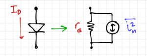
Shot noise is the random movement of quantized charges flowing through a forward-biased PN junction. The shot noise power in a diode, over a unit bandwidth , shown in Fig. 1, is given by:
-
(1)
-
Where , is the DC current flowing through the diode. Shot noise has a white power spectral density similar to thermal noise, however, it is independent of temperature and instead, is proportional to the DC diode current. Since noise, in general, can be considered a "small signal", we normally include the noise generators in the diode small signal model, where is the diode small signal equivalent resistance.
BJT Noise
In a bipolar junction transistor (BJT), both PN junctions produce shot noise. The noise at the base-emitter junction is:
-
(2)
-
And similarly, for the collector-base junction, we get:
-
(3)
-
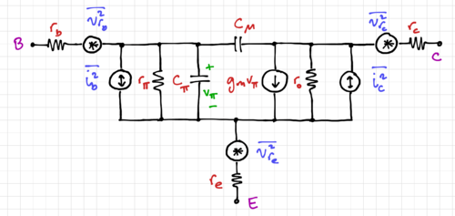
Fig. 2 shows the small signal model of the BJT, showing the shot noise generators, and , and the thermal noise generators for the physical terminal resistances, , , and .
Note that the small signal resistances and are not physical resistors. These small signal resistors are used to model mechanisms such as recombination and base-width modulation, and thus, do not generate noise.
MOSFET Noise
The MOSFET has two noise mechanisms present: (1) thermal noise due to the channel and terminal resistances, and (2) flicker noise due to vacant energy levels or surface states or traps in the interface between the channel and the gate oxide layer. These surface states trap charges for a short period of time, and is then released, producing random changes in the current. Since the probability of charges getting trapped in these surface states is (approximately) inversely proportional to frequency, flicker noise is also known as noise.
We can then express the drain current noise of a MOSFET as the sum of the thermal noise and flicker noise components, over a bandwidth of , respectively:
-
(4)
-
Note that is known as the excess noise coefficient, and is equal to for long channel devices, is the drain-source conductance in the triode region, is the oxide capacitance, and is the effective length of the MOSFET. The constants , , and are process dependent, and are usually determined empirically. In most cases, using is not very convenient. For long channel devices with :
-
(5)
-
This allows us to use the transconductance instead. However, for short-channel devices, . To correct for this, we can introduce a new parameter , leading to an alternative expression for the drain current noise:
-
(6)
-
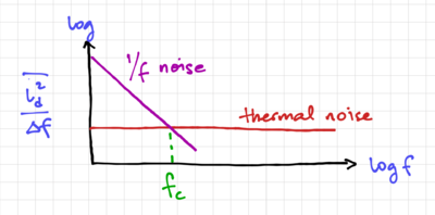
Fig. 3 shows the power spectral density of the MOSFET drain current noise. Note that the spectral density of flicker noise is not white since there is more power in the lower frequencies, thus the term pink noise in reference to the low frequency colors of the visible electromagnetic spectrum. Since the spectral density is not white, we cannot just multiply the spectral density with the bandwidth , but instead, we need to integrate over to get the total area under the spectral density curve. The noise spectral density in a narrow frequency band is also called spot noise. Another useful metric is the flicker noise corner, in Fig. 3, and it is defined as the frequency when the thermal noise component is equal to the flicker noise component. Below the flicker noise corner frequency, flicker noise dominates, while above , thermal noise dominates.
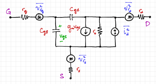
The small signal model of the MOSFET, including the noise generators, is shown in Fig. 4. Once again, physical resistors like the terminal resistances , , and generate noise, while the output impedance, , does not. In RF applications, we are mostly interested in and .


