Difference between revisions of "CoE 197U The CMOS Inverter"
Jump to navigation
Jump to search
| Line 16: | Line 16: | ||
{| | {| | ||
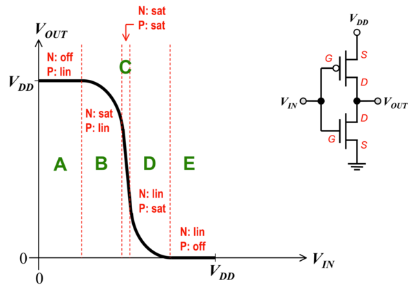
| − | |[[File:Cmos inv vtc.png|thumb|600px|Figure : The CMOS inverter voltage transfer characteristic (VTC)<ref name="king2003">Tsu-Jae King's UCB EECS40 (Fall 2003) Lecture 26 Slides ([https://inst.eecs.berkeley.edu/~ee40/fa03/lecture/lecture26.pdf link]) | + | |[[File:Cmos inv vtc.png|thumb|600px|Figure : The CMOS inverter voltage transfer characteristic (VTC)<ref name="king2003">Tsu-Jae King's UCB EECS40 (Fall 2003) Lecture 26 Slides ([https://inst.eecs.berkeley.edu/~ee40/fa03/lecture/lecture26.pdf link])</ref>.]] |
|- | |- | ||
|} | |} | ||
Revision as of 18:24, 5 March 2021
Contents
The Inverter Voltage Transfer Characteristics (VTC)
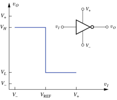
The Ideal Inverter VTC
 Figure : The ideal inverter voltage transfer characteristic (VTC)[1]. |
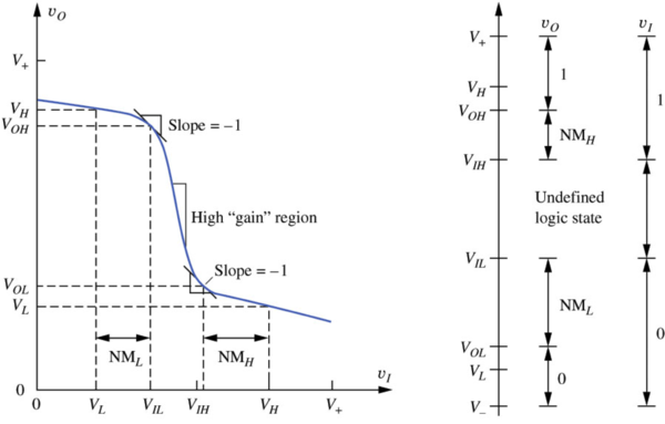
Static Design Metrics
 Figure : The non-ideal inverter voltage transfer characteristic (VTC)[1]. |
 Figure : The CMOS inverter voltage transfer characteristic (VTC)[2]. |
Noise in Digital Circuits
Noise Rejection
Noise Margins
The Regenerative Property of Inverters
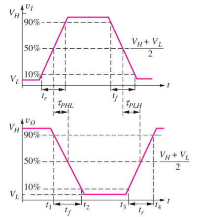
Inverter Delay
 Figure: Logic delay definitions [1]. |