Difference between revisions of "Noise in RF Circuits"
| (28 intermediate revisions by the same user not shown) | |||
| Line 1: | Line 1: | ||
| − | In this module, we consider the noise generated by the electronic devices themselves due to the (1) random motion of electrons due to thermal energy and (2) the discreteness of electric charge. We see this as '''thermal noise''' in resistances, and '''shot noise''' in PN junctions. | + | In this module, we consider the noise generated by the electronic devices themselves due to the (1) random motion of electrons due to thermal energy and (2) the discreteness of electric charge. We see this as '''thermal noise''' in resistances, and '''shot noise''' in PN junctions. In MOS transistors, we also see '''flicker noise'''. This noise is not fundamental, but is due to the way MOS transistors are manufactured, This added uncertainty in the voltages and currents limit the smallest signal amplitude or power that our circuits can detect and/or process, limiting the transmission range and power requirements for reliable communications. Note that purely reactive elements, i.e. ideal inductors and capacitors, do not generate noise, but they can shape the frequency spectrum of the noise. |
== Modeling Noise == | == Modeling Noise == | ||
| Line 26: | Line 26: | ||
=== Noise Power Spectrum === | === Noise Power Spectrum === | ||
| + | [[File:White noise spectrum.png|thumb|300px|Figure 3: The power spectral density of white noise.]] | ||
We can also examine the noise in the frequency domain, specifically, how noise power is distributed over frequency. Many noise sources are ''white'', i.e. the noise power is distributed evenly across all frequencies, as seen in Fig. 3. Thus, white noise is totally unpredictable in time since there is no correlation between the noise at time <math>t_1</math> and the noise at time <math>t_1 + \delta</math>, no matter how small <math>\delta</math> is, since the likelihood of a high frequency change (small <math>\delta</math>) and a low frequency change (large <math>\delta</math>) are the same. | We can also examine the noise in the frequency domain, specifically, how noise power is distributed over frequency. Many noise sources are ''white'', i.e. the noise power is distributed evenly across all frequencies, as seen in Fig. 3. Thus, white noise is totally unpredictable in time since there is no correlation between the noise at time <math>t_1</math> and the noise at time <math>t_1 + \delta</math>, no matter how small <math>\delta</math> is, since the likelihood of a high frequency change (small <math>\delta</math>) and a low frequency change (large <math>\delta</math>) are the same. | ||
| − | The noise power should be the same, whether we obtain it from the time or frequency domain, we | + | The noise power should be the same, whether we obtain it from the time or frequency domain. Thus, calculating the noise power in time and in frequency, and equating the two, we get: |
{{NumBlk|::|<math>\int_0^\infty S_n\!\left(f\right) df = \lim_{T\rightarrow \infty}\frac{1}{T}\int_0^T v^2_n\!\left(t\right) dt</math>|{{EquationRef|5}}}} | {{NumBlk|::|<math>\int_0^\infty S_n\!\left(f\right) df = \lim_{T\rightarrow \infty}\frac{1}{T}\int_0^T v^2_n\!\left(t\right) dt</math>|{{EquationRef|5}}}} | ||
| Line 45: | Line 46: | ||
== Noise Figure == | == Noise Figure == | ||
| + | [[File:RF source with noise.png|thumb|350px|Figure 4: A "noisy" RF source.]] | ||
The noise figure (NF) measures the degradation of SNR in a circuit or block. The noise figure is defined as: | The noise figure (NF) measures the degradation of SNR in a circuit or block. The noise figure is defined as: | ||
| − | {{NumBlk|::|<math> | + | {{NumBlk|::|<math>F=\frac{\mathrm{SNR_{in}}}{\mathrm{SNR_{out}}}</math>|{{EquationRef|7}}}} |
Expressed in dB, we get: | Expressed in dB, we get: | ||
| Line 53: | Line 55: | ||
{{NumBlk|::|<math>\mathrm{NF}=10\log\frac{\mathrm{SNR_{in}}}{\mathrm{SNR_{out}}}</math>|{{EquationRef|8}}}} | {{NumBlk|::|<math>\mathrm{NF}=10\log\frac{\mathrm{SNR_{in}}}{\mathrm{SNR_{out}}}</math>|{{EquationRef|8}}}} | ||
| − | We | + | We use <math>F</math> and <math>\mathrm{NF}</math> to distinguish between the dB and non-dB values of noise figure. Note that some texts call <math>F</math> the ''noise factor''. In measuring or calculating the noise figure, we specify a standard input noise level, generated by a source resistance, <math>R_S</math>, at a set temperature. For example, in RF systems, we typically set <math>R_S=50\mathrm{\Omega}</math> and <math>T=293\mathrm{K}</math>, as seen in Fig. 4. More on this when we cover the origins of electronic noise. |
| − | + | === Amplifier Noise Figure === | |
| + | [[File:Noise amp model.png|thumb|350px|Figure 5: A "noisy" amplifier.]] | ||
| + | Consider the amplifier model in Fig. 5, with input signal <math>S_i</math>, power gain <math>G</math>, and output signal <math>S_o</math>. If the power of the input signal is <math>P_\mathrm{signal}</math>, and <math>N_S</math> is the noise power at the input, we can write the input SNR as: | ||
| + | |||
| + | {{NumBlk|::|<math>\mathrm{SNR_{in}}=\frac{P_\mathrm{signal}}{N_S}</math>|{{EquationRef|9}}}} | ||
| + | |||
| + | Since amplifier will amplify both the signal and the noise, the output SNR is then: | ||
| + | |||
| + | {{NumBlk|::|<math>\mathrm{SNR_{out}}=\frac{G\cdot P_\mathrm{signal}}{G\cdot N_S + N_\mathrm{amp,o}} = \frac{P_\mathrm{signal}}{N_S + \frac{N_\mathrm{amp,o}}{G}} = \frac{P_\mathrm{signal}}{N_S + N_\mathrm{amp,i}}</math>|{{EquationRef|10}}}} | ||
| + | |||
| + | Where <math>N_\mathrm{amp,o}</math> is the noise power at the output of the amplifier when there is no input, and <math>N_\mathrm{amp,i}=\tfrac{N_\mathrm{amp,o}}{G}</math> is the ''input referred'' noise of the amplifier. The noise figure is then: | ||
| + | |||
| + | {{NumBlk|::|<math>F=\frac{\mathrm{SNR_{in}}}{\mathrm{SNR_{out}}}=\frac{P_\mathrm{signal}}{N_S}\cdot\frac{N_S + N_\mathrm{amp,i}}{P_\mathrm{signal}}=1+\frac{N_\mathrm{amp,i}}{N_S} \geq 1</math>|{{EquationRef|11}}}} | ||
| − | = | + | Thus, any real system adds noise and degrades the SNR, resulting in a noise figure greater than one. We only get <math>F=1</math> if we have a noiseless amplifier. |
=== Noise Figure of Cascaded Blocks === | === Noise Figure of Cascaded Blocks === | ||
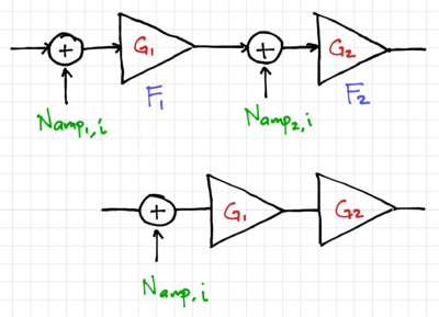
| + | [[File:Cascaded amp noise.png|thumb|400px|Figure 6: Noise in cascaded amplifiers.]] | ||
| + | Two amplifiers are cascaded as shown in Fig. 6. Assume that the amplifiers are properly matched such that the overall power gain is <math>G=G_1\cdot G_2</math>, with noise figures <math>F_1=1+\tfrac{N_{\mathrm{amp_1,i}}}{N_S}</math> and <math>F_2=1+\tfrac{N_{\mathrm{amp_2,i}}}{N_S}</math>. Thus, the input referred noise of amplifier 2 is: | ||
| + | |||
| + | {{NumBlk|::|<math>N_\mathrm{amp_2,i} = N_S \left(F_2 - 1\right)</math>|{{EquationRef|12}}}} | ||
| + | |||
| + | And the total input referred noise is composed of the input referred noise of amplifier 1 plus the noise of amplifier 2 divided by the power gain of amplifier 1: | ||
| + | |||
| + | {{NumBlk|::|<math>N_\mathrm{amp,i} = N_\mathrm{amp_1,i} + \frac{N_\mathrm{amp_2,i}}{G_1} = N_S \left(F_1 - 1\right) + \frac{N_S \left(F_2 - 1\right)}{G_1}</math>|{{EquationRef|13}}}} | ||
| + | |||
| + | Thus, the overall noise figure is: | ||
| + | |||
| + | {{NumBlk|::|<math>F = 1 + \frac{N_\mathrm{amp,i}}{N_S} = 1+ \left(F_1 - 1\right) + \frac{\left(F_2 - 1\right)}{G_1} = F_1 + \frac{F_2 -1}{G_1}</math>|{{EquationRef|14}}}} | ||
| + | |||
| + | In general, for <math>m</math> cascaded amplifiers, the overall noise figure is: | ||
| + | |||
| + | {{NumBlk|::|<math>F = F_1 + \frac{F_2 -1}{G_1} + \frac{F_3 -1}{G_1 G_2} + \frac{F_4 -1}{G_1 G_2 G_3} + \ldots + \frac{F_m -1}{G_1 G_2 \cdots G_{m-1}}</math>|{{EquationRef|15}}}} | ||
| + | |||
| + | This is known as ''Friis' Equation''. Thus, the noise contribution of each successive stage is progressively smaller. This makes the noise of the first stage the dominant noise source, and hence, the most important. | ||
Latest revision as of 09:35, 11 October 2020
In this module, we consider the noise generated by the electronic devices themselves due to the (1) random motion of electrons due to thermal energy and (2) the discreteness of electric charge. We see this as thermal noise in resistances, and shot noise in PN junctions. In MOS transistors, we also see flicker noise. This noise is not fundamental, but is due to the way MOS transistors are manufactured, This added uncertainty in the voltages and currents limit the smallest signal amplitude or power that our circuits can detect and/or process, limiting the transmission range and power requirements for reliable communications. Note that purely reactive elements, i.e. ideal inductors and capacitors, do not generate noise, but they can shape the frequency spectrum of the noise.
Contents
Modeling Noise
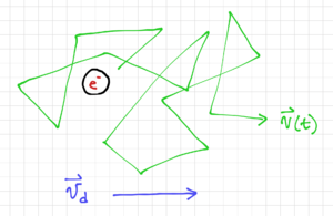
Since electronic noise is random, we cannot predict its value at any given time. However, we can describe noise in terms of its aggregate characteristics or statistics, such as its probability distribution function (pdf). As expected from the Central Limit Theorem, the pdf of the random movement of many electrons would approach a Gaussian distribution with zero mean since the electrons will move around instantaneously, but without any excitation, it will, on the average, stay in the same point in space. If we add an electric field, then the electron will move with an average drift velocity, , but at any point in time, it would be moving with an instantaneous velocity , as shown in Fig. 1. Note that is the electron mobility.
Noise Power
Aside from the mean, to describe a zero-mean Gaussian random variable, , we need the variance, , or the mean of . For random voltages or currents, , this is equal to the average power over time, normalized to :
-
(1)
-
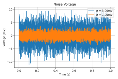
Thus, to describe noise, we can use its variance, or equivalently its average power. Fig. 2 illustrates the difference between two noise signals with different variances. Recall that , the square root of the variance, is the standard deviation.
Consider a noise voltage in time, , similar to the ones depicted in Fig. 2. The mean is then:
-
(2)
-
The variance, however, is non-zero:
-
(3)
-
We can also calculate the root-mean-square or RMS as:
-
(4)
-
Noise Power Spectrum
We can also examine the noise in the frequency domain, specifically, how noise power is distributed over frequency. Many noise sources are white, i.e. the noise power is distributed evenly across all frequencies, as seen in Fig. 3. Thus, white noise is totally unpredictable in time since there is no correlation between the noise at time and the noise at time , no matter how small is, since the likelihood of a high frequency change (small ) and a low frequency change (large ) are the same.
The noise power should be the same, whether we obtain it from the time or frequency domain. Thus, calculating the noise power in time and in frequency, and equating the two, we get:
-
(5)
-
Where is the noise power spectral density in . An alternate representation of the noise spectrum is the root spectral density, , with units of .
Noise in Communication Systems
Noise is present in all parts of a communication system. In analog systems, it reduces the quality of the received signal, e.g. introducing static sounds in audio signals, or "snow" in television images. In digital systems, it degrades throughput, e.g. due to retransmissions caused by packet errors or the due to the extra coding needed to recover data in the presence of errors.
Signal-to-Noise Ratio
In general, we try to maximize the signal-to-noise ratio (SNR) in a communication system. For an average signal power , and an average noise power , the SNR in dB is defined as:
-
(6)
-
Again note that we are referring to random noise and not interference or distortion.
Noise Figure
The noise figure (NF) measures the degradation of SNR in a circuit or block. The noise figure is defined as:
-
(7)
-
Expressed in dB, we get:
-
(8)
-
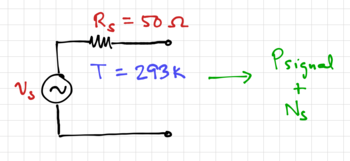
We use and to distinguish between the dB and non-dB values of noise figure. Note that some texts call the noise factor. In measuring or calculating the noise figure, we specify a standard input noise level, generated by a source resistance, , at a set temperature. For example, in RF systems, we typically set and , as seen in Fig. 4. More on this when we cover the origins of electronic noise.
Amplifier Noise Figure
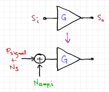
Consider the amplifier model in Fig. 5, with input signal , power gain , and output signal . If the power of the input signal is , and is the noise power at the input, we can write the input SNR as:
-
(9)
-
Since amplifier will amplify both the signal and the noise, the output SNR is then:
-
(10)
-
Where is the noise power at the output of the amplifier when there is no input, and is the input referred noise of the amplifier. The noise figure is then:
-
(11)
-
Thus, any real system adds noise and degrades the SNR, resulting in a noise figure greater than one. We only get if we have a noiseless amplifier.
Noise Figure of Cascaded Blocks
Two amplifiers are cascaded as shown in Fig. 6. Assume that the amplifiers are properly matched such that the overall power gain is , with noise figures and . Thus, the input referred noise of amplifier 2 is:
-
(12)
-
And the total input referred noise is composed of the input referred noise of amplifier 1 plus the noise of amplifier 2 divided by the power gain of amplifier 1:
-
(13)
-
Thus, the overall noise figure is:
-
(14)
-
In general, for cascaded amplifiers, the overall noise figure is:
-
(15)
-
This is known as Friis' Equation. Thus, the noise contribution of each successive stage is progressively smaller. This makes the noise of the first stage the dominant noise source, and hence, the most important.
