Difference between revisions of "EEE 51 Transistor Models"
| Line 12: | Line 12: | ||
==== The BJT Transfer Characteristic ==== | ==== The BJT Transfer Characteristic ==== | ||
| − | [[File:Common-emitter_config. | + | [[File:Common-emitter_config.pdf|thumb|right|250px|Figure 1: The BJT common-emitter configuration.]] |
The BJT common-emitter (CE) configuration is shown in Fig. 1. We define the “input” signal as the base-emitter voltage, <math>V_{BE}</math>, and the “output” signal as the collector current <math>I_{C}</math>. Therefore, we can model the the BJT transfer characteristic using | The BJT common-emitter (CE) configuration is shown in Fig. 1. We define the “input” signal as the base-emitter voltage, <math>V_{BE}</math>, and the “output” signal as the collector current <math>I_{C}</math>. Therefore, we can model the the BJT transfer characteristic using | ||
Revision as of 00:14, 20 June 2020
In EEE 41, you studied the fundamental concepts of how transistors can be realized using semiconductors, specifically, the two most popular transistors currently in use: the bipolar junction transistor (BJT) and the metal-oxide field-effect transistor (MOSFET).
In EEE 51, we want to be able to use these transistors (as well as other semiconductor devices such as diodes) to design and implement useful electronic circuits. This means we have to be able to describe, and eventually predict, the behavior of the terminal voltages and currents of these devices. We can accomplish this by using transistor models.
Contents
Large Signal Transistor Models
The large signal transistor models allow us to describe the electrical behavior of the transistor, when a voltage or current is varied over its allowable range. Here, we can see how varying the terminal voltages (and currents) determine the operating region of the transistor. Since there are many combinations of voltages and currents available for us to choose from, it is convenient to standardize which terminal voltages/currents we can use. This makes it easy to compare different transistors, as well as to systematically analyze and design electronic circuits based on these transistors.
The standard large signal transistor characteristics that we use are (1) the transfer characteristics, (2) the output characteristics, and (3) the input characteristics. Note that these models are normally considered as DC or low-frequency models, where we assume that the transistor parasitic capacitances are still negligible.
Transfer Characteristics
Transfer characteristics usually implies an input-output relationship, similar to the transfer function of a two-port network. But where are the input/output terminals or ports of a transistor? As we will see later on, one of the main goals of electronic circuits is to amplify signals (i.e. voltage, current, etc). Thus, it is convenient to choose the input-output terminal pair of a transistor that is commonly used to provide the largest amplification. In the BJT case, it is the common-emitter configuration, and in the MOSFET case, it is the common-source configuration.
The BJT Transfer Characteristic
The BJT common-emitter (CE) configuration is shown in Fig. 1. We define the “input” signal as the base-emitter voltage, , and the “output” signal as the collector current . Therefore, we can model the the BJT transfer characteristic using
-
(1)
for a transistor in the forward-active region.[fn 1] Note that is the reverse saturation current of the collector-base junction and dependent on the type and geometry of the transistor, is the ideality factor, accounting for recombination in the base-emitter junction, is the Early Voltage, and , the voltage equivalent of temperature ( at ). For typical discrete (not integrated) BJTs, the value of is around , and since is normally in the tens of volts, we can simplify Eq. (1) into
-
(2)
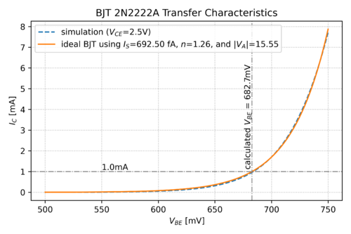
Eq. (1), shown in Fig. 2, and superimposed with the transfer characteristic of a real BJT, allows us to approximate the behavior of the “output” signal, in this case the collector current, when we change the base-emitter voltage, our “input” signal.
The MOSFET Transfer Characteristic
The MOSFET common-source (CS) configuration is shown in Fig. 3. As with the BJT, we define the “input” signal as the gate-source voltage, , and the “output” signal as the drain current, . Thus, the MOSFET transfer characteristic can be modeled as
-
(3)
in the saturation region.[fn 2] Note that is a constant dependent on the technology used in the manufacture, and the geometry, of the transistor, is the transistor threshold voltage, and is the channel length modulation coefficient. For typical discrete (not integrated) MOSFETs, , allowing us to approximate Eq. (3) with
-
(4)
Notes
- ↑ In EEE 51, we will almost always use the BJT in the forward active region. However, in circuits where this is not the case, the transfer characteristic should be modeled with the appropriate relationship between and .
- ↑ In EEE 51, we will almost always use the MOSFET in the saturation region. However, in circuits where this is not the case, the transfer characteristic should be modeled with the appropriate relationship between and .


