SFG Butterworth Low-Pass Filter Example
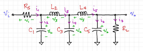
A 5th-order passive low-pass Butterworth filter is shown in Fig. 1. For and , we get , , and . To convert this passive RLC filter into its active equivalent, we need to first label all the voltages and currents.
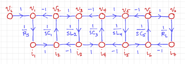
We can then express the capacitor voltages in terms of its currents to get the integrator form for . Similarly for the inductor currents, we get for . With the remaining KCL and KVL equations, we can construct the signal flow graph in Fig. 2.
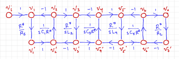
Using a normalizing resistor, , we can normalize the signal flow graph in Fig. 2 to convert the current nodes into voltage nodes.
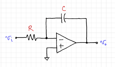
After normalization, we can then convert the signal flow graph directly to its equivalent integrator-based circuit, shown in Fig. 4.
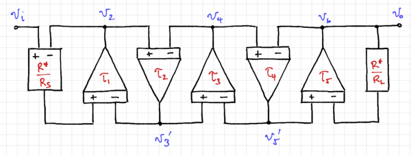
Each integrator can then be implemented using op-amps, as shown in Fig. 5.
Note that:
-
(1)
-
For , and
-
(2)
-
For . If we choose , we then get the capacitor values for the integrator in Fig. 5 as , , and . However, notice that the integrators require a subtraction at its inputs. We can add amplifiers with a gain of , but this may not be the best solution.
We can solve this problem by using fully differential amplifiers and integrators.
Differential Integrators
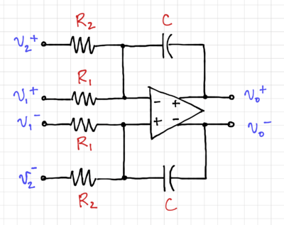
One way to address the need for addition and subtraction is to use fully differential amplifiers, where both inverting and non-inverting paths are already generated, and multiplying a signal by can be done by simply re-labeling the outputs, i.e. swapping the label for and . We can then convert the two-input single-ended integration in Fig. 6, with output voltage:
-
(3)
-
Into its fully-differential equivalent, as shown in Fig. 7 with an output voltage equal to:
-
(4)
-
Note that swapping and is equivalent to multiplying the output by , allowing us to perform both addition and subtraction. Additionally, using fully differential circuits reduces power supply noise and increases common-mode rejection.
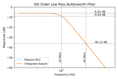
Using fully differential integrators, we can now construct the active filter, and using this SPICE file, we get the magnitude response in Fig. 8. Note that the first integrator, with time constant , needs three inputs to accommodate , , and . All the other integrators have two-inputs. As expected, the integrator-based active filter matches the response of the passive RLC circuit perfectly.
Maximizing Dynamic Range
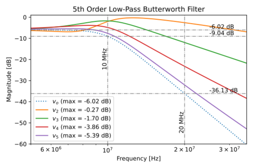
We can plot the intermediate internal nodes of the active filter, i.e. the outputs of the integrators, as shown in Fig. 9. Notice that the required maximum voltage swings of these nodes differ by quite a bit. Amplifiers with lower maximum output swings will have lower signal-to-noise ratios (SNR), and if the output swings are different, we will need to design and optimize the integrators individually.
Since we are using amplifiers, we can control the gain of the integrators, and scale the output voltage of the individual amplifiers such that: (1) we maximize the output swing of each amplifier/integrator, and hence the dynamic range/SNR, and (2) make the output swings of all the integrators equal to each other, so we can just use one specification in designing all the integrators, reducing the design effort. Scaling the output node by a factor of gives us:
-
(4)
-
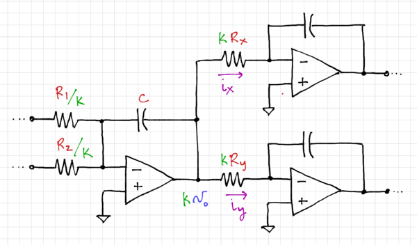
Note that we also have to scale the resistances of the load integrators by to maintain the same currents and so that the output swings of these downstream integrators are maintained, as shown in Fig. 10. Thus, Similar to scaling the nodes in a SFG, to scale the integrator output by a factor of , we need to scale the integrator resistances by , and scale the resistance of the load integrators by a factor of .
Fig. 11 shows the magnitude response of the intermediate nodes after scaling using this SPICE file. Again, because of the presence of active elements, i.e. amplifiers, we can scale the output node as well, as shown in Fig. 12, and generated using this SPICE file.
In this example, we scaled all the integrator outputs to have a maximum swing of 1 (0 dB) relative to the input, but in general we can scale it to have even more gain depending on the application and implementation constraints.
Noise Analysis
Recall from our review of integrators that if we assume the noise of the resistors dominate, the total output integrated noise of the three-input integrator is equal to:
-
(5)
-
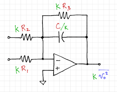
In our example, the total RMS noise voltage is simulated to be . Depending on the application, this could sufficient, too small, or too large. Consider the case when this noise is too small for our purposes. We can scale the noise up by reducing the capacitance value. To maintain the same integrator time constant, we need to scale the resistors up by the same factor, as seen in Fig. 13.
So if we want to scale up the noise to , we need to scale the capacitors by:
-
(6)
-
Note that scaling the noise to the appropriate level can significantly lower the capacitor values and increase the resistance values, saving significant chip area and power, as well as reducing the effect of parasitic elements.


