CoE 197U CMOS Inverter
To understand the analysis and design of digital circuits, we will look at its fundamental element -- the digital gate. We will start with the simplest digital gate, the inverter, and look at the basic functionality, static metrics, delay, power, and energy characteristics of CMOS inverters.
Contents
The Inverter Voltage Transfer Characteristics (VTC)
The functionality of the inverter can be captured by looking at the output voltage as we change the input voltage, or the voltage-transfer characteristic (VTC).
The Ideal Inverter VTC
Let us define an ideal inverter, where:
-
(1)
-
Where is logic 1 voltage level, and in general may or may not be equal to the positive supply voltage, , and is logic 0 voltage level, and in general may or may not be equal to the negative supply voltage, . The VTC of this ideal inverter, as well as the standard inverter circuit symbol, is shown in Fig. 1.
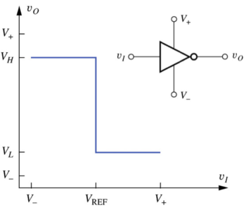 Figure 1: The ideal inverter voltage transfer characteristic (VTC)[1]. |
Inverter Implementations
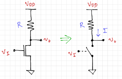
One implementation of the inverter is to use a single NMOS transistor and a resistor, as shown in Fig. 2. Using our switch model for the NMOS transistor, we can see that when the input is low or at logic 0, the output is pulled up to since the switch is open. When the input voltage is equal to , the switch is closed and the output is pulled down close to ground. For a finite on switch resistance, , the output voltage becomes:
-
(2)
-
Note that a finite will degrade (increase) low output voltage or logic 0 level. Additionally, the when the output of the NMOS inverter is low, there is a non-zero current flowing through the resistor, resulting in static power consumption, or power consumed from the supply even when there is no switching activity present in the circuit.
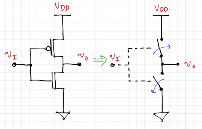
Another implementation of the inverter is to use an NMOS and a PMOS transistor. This complementary (CMOS) configuration turns on only one switch at a time since the gates of the two transistors are connected to each other. Thus, an input voltage of will turn on (close) the NMOS switch, and turn off (open) the PMOS switch since the gate-to-source voltage of the PMOS transistor is zero, pulling the inverter output down to ground. When the input voltage is ground or logic 0, the NMOS switch is open and the PMOS is closed, pulling the output up to .
Note that due to the complementary function of the CMOS inverter, there is no static current flowing when the output is either at logic 0 or logic 1. However, current will flow during the transition from 01 or 10.
We can derive the VTC of any inverter by determining the regions of operation of each transistor as we vary the input voltage. Fig. 4 shows the VTC of the CMOS inverter with the corresponding regions of operation, which are dependent on the input and output voltages. Note that:
- .
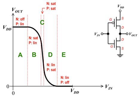 Figure 4: The CMOS inverter voltage transfer characteristic (VTC)[2]. |
Static Design Metrics
The general form of the inverter voltage transfer characteristic is shown in Fig. 5. We can define several metrics to enable us to determine how close the real VTC is to the ideal VTC.
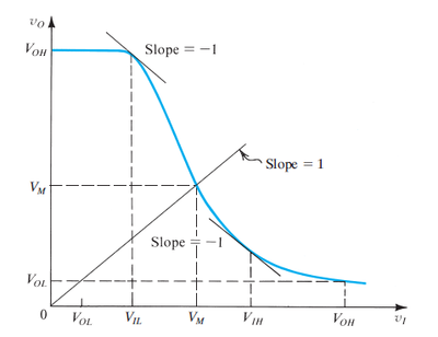 Figure 5: The non-ideal inverter voltage transfer characteristic (VTC)[3]. |
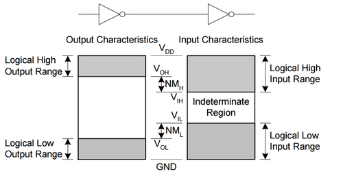 Figure 6: Noise margin definitions[4]. |
Let us define the following basic inverter VTC features:
- is the nominal output high or logic 1 output of the inverter, and is seen at the output when or logic 0 is placed at the input of the inverter.
- is the nominal output low or logic 0 output of the inverter, and is seen at the output when or logic 1 is placed at the input of the inverter.
- If we connect the output of the inverter to its input, then we would expect the voltage to settle at the point where , or the midpoint voltage. Graphically, this can be determined by drawing a 45-degree line on the VTC curve, as shown in Fig. 5.
In the ideal inverter VTC in Fig. 1, we see that we have two flat regions (zero gain) and a vertical region (infinite gain). However, in a non-ideal VTC, the zero gain regions degrade into low gain regions where the absolute value of the slope is typically less than 1, and a high-gain region where the absolute value of the slope is greater than 1. The boundaries between the high- and low-gain regions are marked by the points where the absolute value of the slope of the VTC is equal to 1.
The two points with a slope of are shown in Fig. 5, where is the highest input voltage the inverter will still consider as a low voltage. Anything above this places the inverter in the high-gain region of the VTC, making it sensitive to noise and interference. Similarly, is the lowest input voltage the inverter will still consider as a high voltage.
Noise in Digital Circuits
One of the main advantages of digital circuits over analog circuits is its relatively good noise immunity. In a binary digital logic system, we reduce the amount of information carried by a digital signal to just 1 bit. This then increases the digital circuit's robustness to interference from nearby signals, or from inherent device noise. The zero-gain regions of the ideal inverter VTC are ideal at the points near and since any disturbance or noise added to the input voltage would just be ignored by the inverter, i.e. the output voltage will not change.
Noise Margins
To quantify this robustness to noise and interference, we define the following metrics as illustrated in Fig. 6:
- is the noise margin at the high output level, and is the maximum noise that can reduce the input high or logic 1 level to the point where the inverter might not recognize it as a high level anymore.
- is the noise margin at the low output level, and is the maximum noise that can increase the input low or logic 0 level to the point where the inverter might not recognize it as a low level anymore.
Note that input signals between and are considered to be in the indeterminate or undefined region, where because of the high gain, small variations in the input could result in large output variations, possibly leading to erroneous inverter outputs.
The Regenerative Property of Inverters
It is desirable to have a VTC with two low-gain regions, at the nominal input and output voltages, that are separated by a high-gain region. An inverter with this type of VTC is called a regenerative inverter. This means that if a signal is degraded by noise, leaving it in the indeterminate or undefined zone, then by passing this signal into a chain of inverters, the signal will eventually approach one of the nominal voltage levels, as seen in Fig. 7.
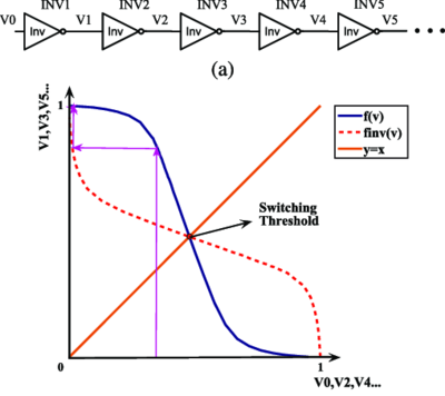 Figure 7: The regenerative property of cascaded inverters[5]. |
Inverter Delay
Aside from the static metrics, we also have the inverter dynamic characteristics, or what happens to the inverter when the input changes from high to low, or low to high. Specifically, we are interested in the time it takes for the output to settle to its correct value once the input has changed.
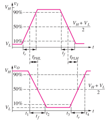 Figure 8: Logic delay definitions [1]. |
To easily compare delays, we use the standard delay definitions in Fig. 8.
- The rise time, , is defined as the time it takes for a 01 transition to go from 10% to 90% of its voltage swing.
- The fall time, , is defined as the time it takes for a 10 transition to go from 90% to 10% of its voltage swing.
- The propagation delay, is defined as the time interval between the time the input reaches 50% of its voltage swing to the time the output reaches 50% of its voltage swing. Since the propagation delay does not have to be the same for a 01 and a 10 output transition, we can evaluate the propagation delay for each of these cases:
- The propagation delay, high-to-low, , is the propagation delay when the output transitions from high to low.
- The propagation delay, low-to-high, , is the propagation delay when the output transitions from low to high.
A Simple CMOS Inverter Delay Model
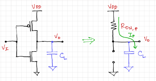
Let us try to estimate the delay of an inverter. First, we recognize that in a purely CMOS digital system, an inverter will drive another CMOS gate, and in this case, let us simplify it to just an inverter. The inverter input impedance is capacitive since we are looking into the gate of both the NMOS and PMOS transistors. Secondly, this output capacitance will be charged by the PMOS transistor when the output transitions from low to high, and it will be discharged by the NMOS when the output goes from high to low. Thus, we can model each transition separately.
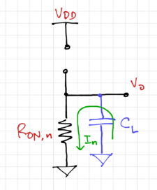
For the low-to-high transition, we can model the CMOS inverter as ON resistance of the PMOS charging the load capacitance as seen in Fig. 9. The high-to-low transition can be modeled in a similar fashion, as shown in Fig. 10.
For the simple RC model, we can easily calculate the output low-to-high step response as:
-
(3)
-
Where . Thus, the propagation delay is the time it takes for the output to reach is:
-
(4)
-
Similarly, the propagation delay from high to low is:
-
(5)
-
Where .
Since the inverter propagation delay is very much dependent on the load capacitance, it is convenient to define a standard capacitance load so we can compare inverters not only of different topologies, but also across different technologies. One convenient way is to get the delay of an inverter with a fan-out of 4 (FO4), or an inverter driving 4 other identical inverters as shown in Fig. 11. Thus, the FO4 inverter delay uses , where is the input capacitance of the inverter.
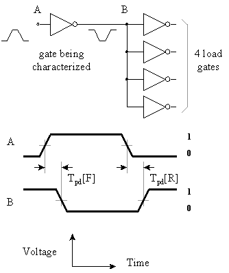 Figure 11: The inverter FO4 delay[6]. |
References
- ↑ Jump up to: 1.0 1.1 Ming Wu's UCB EE105 (Fall 2014) Lecture 24 Slides (link)
- ↑ Tsu-Jae King's UCB EECS40 (Fall 2003) Lecture 26 Slides (link)
- ↑ Electrical Engineering Stack Exchange (link)
- ↑ VLSI Basic Blog (link)
- ↑ Zou, Xuncheng & Nakatake, Shigetoshi, A Low Voltage Stochastic Flash ADC without Comparator, IEICE Transactions on Fundamentals of Electronics, Communications and Computer Sciences, 2019. E102.A. 886-893. 10.1587/transfun.E102.A.886.
- ↑ P. DeMone (link)


