CoE197U 2s2324 Scaling
Contents
Moore's Law
In 1965, Gordon Moore published a 4-page paper entitled Cramming more components onto integrated circuits[1], where he predicted that the number of components in an integrated circuit will increase by a factor of two every year, as shown in Fig. 1. Note that he based his extrapolation on just 4 data points!
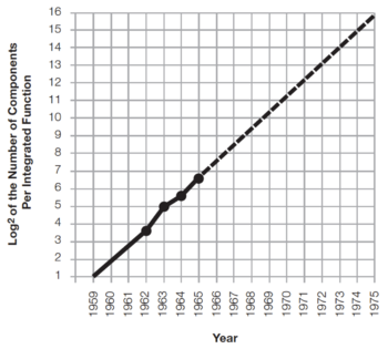 Figure 1: Gordon Moore's 1965 prediction[1]. |
Why is this paper and the graph in Fig. 1 important? Gordon Moore's prediction, also known as Moore's Law, has reflected and, more importantly, driven the steady and rapid progress in computing technology[2]. Thus, satisfying Moore's Law has become the goal instead of being merely a prediction.
Evolution of Complexity
As Gordon Moore predicted, the cost and performance advantage of putting more and more devices into a single integrated circuit (IC) led to the rapid increase in circuit complexity. One convenient indicator of circuit complexity is the number of transistors contained in a single IC, reaching the 1-billion transistor level in 2010, and achieving almost 50 billion transistors in 2020, as shown in Fig. 2.
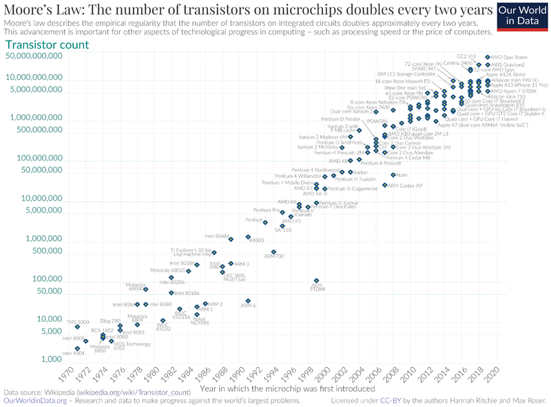 Figure 2: Transistor Count (1970 - 2020)[3]. |
Challenges in Digital Design
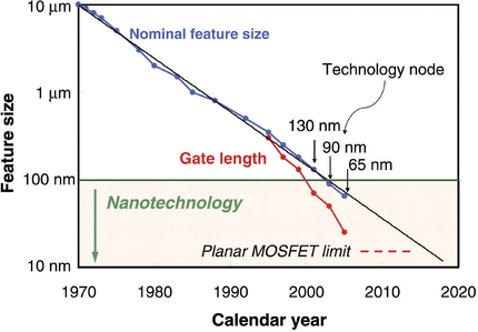
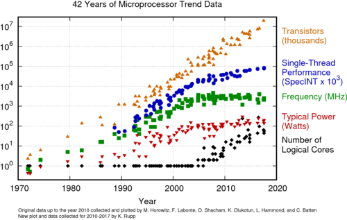
For more than 30 years, the development of integrated circuits continued roughly on the trajectory predicted by Moore's Law. This steady advance has relied heavily on the advances in device and fabrication technologies. Device dimensions are gone down by a factor of approximately 0.7 every generation, giving us approximately a 50% reduction in device area every 2 years, as seen in Fig. 3. However, in the past decade, we have seen a slowdown in the pace of development and performance of integrated circuits, seen in Fig. 4, as we face various physical and manufacturing limitations.
The Power Wall
As MOS device sizes continue to scale, digital gate delays also decrease, leading to higher maximum operating frequencies. This results in higher average dynamic power consumption, , which is proportional to the frequency of operation and the square of the supply voltage, or equivalently:
-
(1)
-
This gives rise to higher power densities or power per unit volume. Since the power is dissipated as heat, adequate cooling mechanisms must be put in place to prevent the temperature from rising to levels that can reduce the performance or cause permanent damage to the IC. In most applications, the additional cooling costs might not be worth the extra performance. Thus, instead of a steady increase as predicted by Moore's Law, clock frequencies are starting to level off, as seen in Fig. 4. As expected, the power and single-core performance also levels off.
Leakage Current
In MOS transistors, the subthreshold current can be expressed as:
-
(2)
-
Thus, even with , the drain current is not zero, but ideally this leakage current is very small compared to the MOS saturation current. The resulting leakage current also increases as the transistor lengths are reduced since the distance between the source and drain regions are also reduced. In deeply scaled technologies, the resulting static power consumed due to leakage current is projected to be comparable or even dominate the total chip power consumption, as shown in Fig. 5. This is problematic since the IC would consume a significant amount of power even when idle, losing one of the original advantages of CMOS over other technologies such as BJTs.
In digital CMOS gates, decreasing the supply voltage decreases the MOS saturation current, leading to increased delays, since:
-
(3)
-
One way to maintain performance is to reduce the MOS threshold voltage, as the supply voltage is reduced. However, lowering the threshold voltage increases the MOS subthreshold leakage current. This power-delay tradeoff prevents the supply and threshold voltages from scaling at the same rate as the device sizes, as seen in Fig. 6.
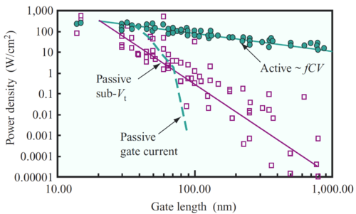 Figure 5: Active and Leakage Power[6]. |
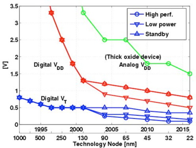 Figure 6: Supply and threshold voltage scaling[7]. |
Why Scale?
The motivation for scaling is centered around cost and performance, enabling us to perform tasks that were previously not possible, or if it were possible before, the cost was very prohibitive. Thus, the semiconductor industry continues to invest in technologies that would continue the scaling of integrated circuits for as long as possible. Fig. 7 shows a possible trajectory of how scaling supports the computing industry in the artificial intelligence field.
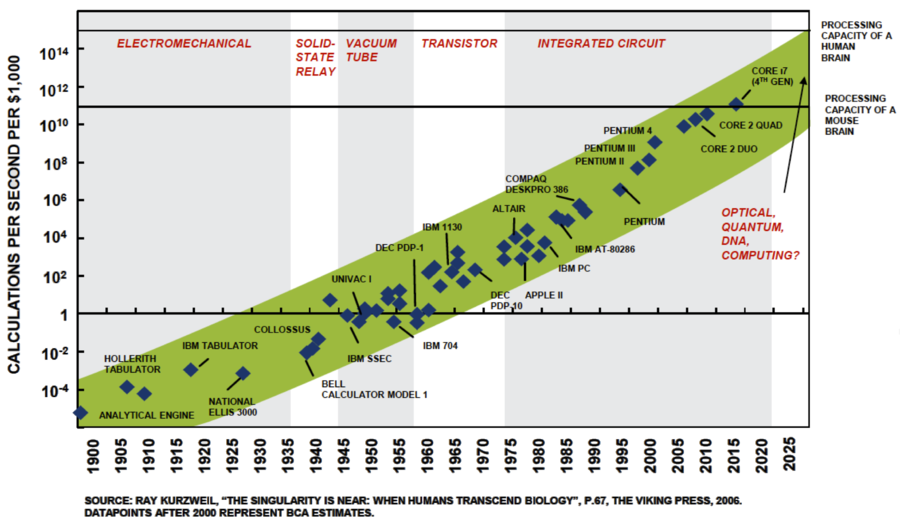 Figure 7: Calculations per second for a fixed cost[8]. |
The Cost of Integrated Circuits
Cost is the main motivation for reducing device sizes. Aside from the marked improvement in speed, more transistors can be integrated in the same die or wafer, and this results in the significant reduction in the cost per transistor. The total cost of producing an integrated circuit can be broken down into two components: (1) the fixed or non-recurrent engineering costs (NRE), and (2) the variable or recurrent costs.
- Non-Recurrent Engineering (NRE) Costs
-
- NRE costs are overhead costs independent of volume, i.e. the number of integrated circuits made or sold.
- Examples of NRE costs include design time and manpower, CAD tools and equipment, mask generation costs, etc.
- Recurrent Costs
-
- Costs that are proportional to the volume of ICs produced.
- This includes the fabrication costs, packaging costs, and testing costs.
- In most cases, these costs are proportional the chip area.
Thus, the cost of an integrated circuit can be expressed as:
-
(4)
-
Where the components of the variable cost are:
-
(5)
-
Die Cost
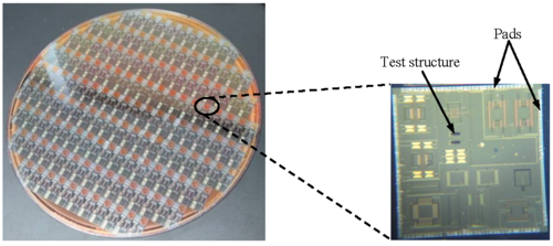
The cost of a die or chip is dependent on the (1) cost of a wafer, shown in Fig. 9, (2) the number of chips or dies in a wafer, and (3) the die yield:
-
(6)
-
Note that increasing the number of dies in a wafer can reduce the cost per die. This can be done by increasing the size of the wafer, as long as the increase in cost due to the larger wafer size is offset by the reduction in overall cost due to more dies in a wafer. However, increasing the wafer size can cause structural problems such as warping of the wafer, leading to increased device variability.
Yield
The yield, , is defined as the ratio of good dies in a wafer relative to the total number of dies in a wafer, or equivalently in percent units:
-
(7)
-
We can estimate the total number of dies, each with area , in a wafer with diameter, as:
-
(8)
-
The first term in Eq. 8 gives us the total wafer area divided by the die area. However, as seen in Fig. 9, there are partial dies at the edge of the wafer that must be discounted since they cannot be used. The number of partial dies at the edge is estimated by the second term in Eq. 8. Note that by reducing the die area, the yield can significantly increase for the same wafer defect pattern, as shown in Fig. 10. Thus, for large die sizes, the die cost is higher since the yield is lower, thus the cost of the good dies must shoulder the cost of the bad dies.
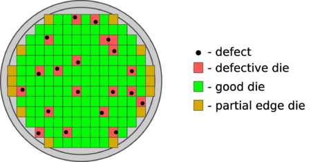 Figure 9: Wafer defects due to fabrication non-idealities[10]. |
 Figure 10: The effect of die size on yield[11]. |
Go to Next topic CoE 197U The MOS Switch
Back to Main Page CoE 197U S2 AY 2023-2024
References
- ↑ Jump up to: 1.0 1.1 Gordon E Moore, Cramming more components onto integrated circuits, Electronics, Volume 38, Number 8, April 19, 1965 (pdf)
- ↑ Gordon Moore: The Man Whose Name Means Progress, IEEE Spectrum, March 2015.
- ↑ Wikimedia
- ↑ S. E. Thompson, S. Parthasarathy, Moore's law: the future of Si microelectronics, Materials Today, Volume 9, Issue 6, 2006, Pages 20-25. (link)
- ↑ K. Rupp, 42 Years of Microprocessor Trend Data, link
- ↑ W. Haensch et al., Silicon CMOS devices beyond scaling, IBM Journal of Research and Development, vol. 50, no. 4.5, pp. 339-361, July 2006, doi: 10.1147/rd.504.0339.
- ↑ ITRS, The International Technology Roadmap for Semiconductors (2004 edition), 2004. Technical Report, http://public.itrs.net
- ↑ BCA Research (link).
- ↑ J. Dennis, CMOS Compatible Bulk Micromachining, IntechOpen 2013 (link)
- ↑ WikiChip (link)
- ↑ K. Choi's lecture notes on Design Metrics, CMPEN 411: VLSI Digital Circuits, Pennsylvania State University, Fall 2016 (link)


